Preparation method of single crystal film bulk acoustic wave resonator and bulk acoustic wave resonator

A bulk acoustic wave resonator, single crystal thin film technology, applied in the manufacture/assembly of piezoelectric/electrostrictive devices, piezoelectric/electrostrictive/magnetostrictive devices, impedance networks, etc., can solve the problem of single crystal thin film layer Problems such as cracks, single-crystal thin-layer film warping, and sags can be achieved to simplify the preparation steps, ensure device performance, and simplify the hole-opening process.

Active Publication Date: 2019-07-12
UNIV OF ELECTRONICS SCI & TECH OF CHINA
View PDF5 Cites 11 Cited by
  • Summary
  • Abstract
  • Description
  • Claims
  • Application Information

AI Technical Summary

Problems solved by technology

[0006] The object of the present invention is to provide a preparation method of a single crystal thin film cavity type bulk acoustic wave resonator and a cavity type bulk acoustic wave resonator, by preparing a conductive material covering the entire lower surface of the single crystal thin film layer on the lower surface of the single crystal thin film layer. The design of the lower electrode with the isolation function solves the problem that during the bonding process, the bubbles generated in the bonding layer cause cracks in the single crystal thin film layer, which makes the single crystal thin film lift up or sag or even break, affecting the cavity type. Technical Issues on the Overall Performance of Bulk Acoustic Wave Resonators

Method used


Image

  • Preparation method of single crystal film bulk acoustic wave resonator and bulk acoustic wave resonator
  • Preparation method of single crystal film bulk acoustic wave resonator and bulk acoustic wave resonator
  • Preparation method of single crystal film bulk acoustic wave resonator and bulk acoustic wave resonator

Examples


preparation example Construction

[0054] Such as figure 1 , figure 2 , image 3 , image 3 , Figure 5 and Figure 6 As shown, the present invention provides a kind of preparation method of monocrystalline thin film bulk acoustic resonator, comprises the steps:

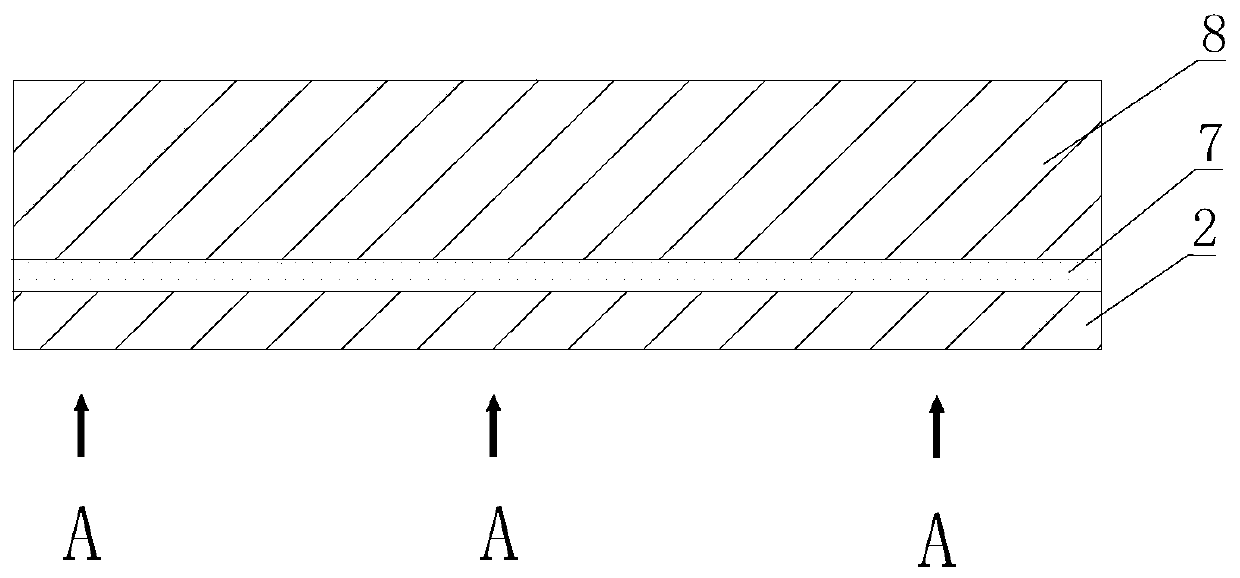
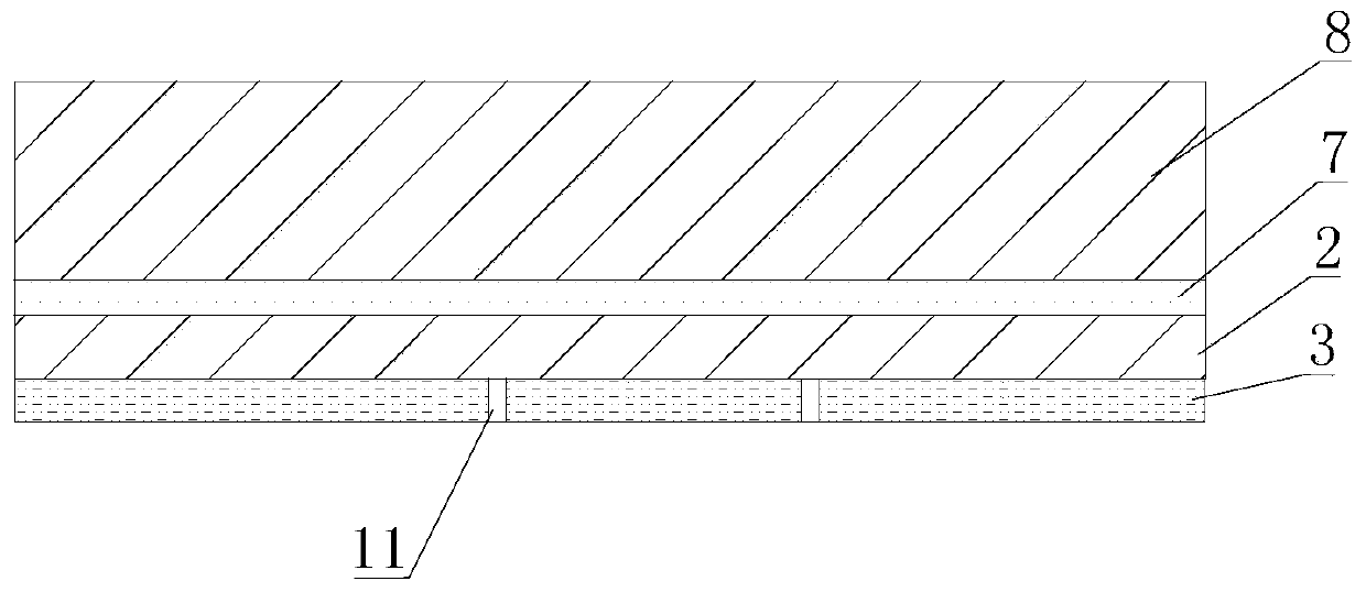
[0055] S1) High-energy ions A are injected from the lower surface of the single-crystal wafer, and the high-energy ions A enter the interior of the single-crystal wafer to form a damaged layer 7, and the single-crystal wafer is separated into an upper piezoelectric layer 8 and a single-crystal thin film layer 2, and the obtained Damaged single crystal wafers;

[0056] S2) Coating photoresist on the lower surface of the damaged single crystal wafer to form a photoresist layer, using a patterned mask to expose and develop the photoresist, growing the lower electrode, preparing the lower electrode, removing photoresist, so that the surface of the grown lower electrode forms a patterned through hole 11 connected to the single crystal thin film laye...

Embodiment 1

[0100] The preparation of a lithium niobate single crystal thin-film cavity-type bulk acoustic wave resonator by method 1 includes the following steps:

[0101] 1) A lithium niobate single crystal wafer is selected, and high-energy helium ions (He 2 +), so that a damage layer is formed inside the lithium niobate single crystal wafer, and the damage layer separates the lithium niobate single crystal wafer into a lithium niobate upper piezoelectric layer and a lithium niobate single crystal film layer; He 2 + The implantation energy is 200keV, and the implantation depth is 0.6μm;

[0102] 2) Coating photoresist (Ruihong AZ6212) on the lower surface of the lithium niobate single crystal thin film layer to form a photoresist layer, and using a patterned mask (made of chromium) to expose and develop the photoresist , grow the Pt lower electrode, and use acetone to clean and remove the photoresist, so that the surface of the grown Pt lower electrode forms a through hole connected w...

Embodiment 2

[0108] The preparation of a lithium tantalate single crystal thin-film cavity-type bulk acoustic wave resonator by method 1 includes the following steps:

[0109] 1) A lithium tantalate single crystal wafer is selected, and high-energy helium ions (He 2 +), so that a damage layer is formed inside the lithium tantalate single crystal wafer, and the damage layer separates the lithium tantalate single crystal wafer into a piezoelectric layer on lithium tantalate and a lithium tantalate single crystal film layer; He 2 + The implantation energy is 500keV, and the implantation depth is 0.6μm;

[0110] 2) Coating photoresist (Ruihong AZ6212) on the lower surface of the lithium tantalate single crystal film layer to form a photoresist layer, and using a patterned mask (made of chromium) to expose and develop the photoresist , grow the Pt lower electrode, and use acetone to clean and remove the photoresist, so that the surface of the grown Pt lower electrode forms a through hole conne...


PUM


Abstract

The invention relates to the technical field of preparation of acoustic resonators, in particular to a preparation method of a single crystal film bulk acoustic resonator and the bulk acoustic resonator. The invention aims to solve problems that by using a preparation method of a single crystal film cavity type bulk acoustic wave resonator, through the design that a lower electrode which covers the lower surface of the whole single crystal thin film layer and has conductive and isolation effects is prepared on the lower surface of the single crystal thin film layer, in a binding process, bubbles generated by the bonding layer cause cracks to be generated on the single crystal film layer, so that the single crystal film layer is warped or sunken or even broken, and the overall performance of the cavity type bulk acoustic wave resonator is influenced.

Description

technical field [0001] The invention relates to the technical field of acoustic wave resonator preparation, in particular to a method for preparing a single crystal thin film bulk acoustic wave resonator and the bulk acoustic wave resonator. Background technique [0002] With the rapid development of wireless communication technology, traditional dielectric filters and surface acoustic wave filters are difficult to meet the high-frequency requirements. The new generation of thin film bulk acoustic resonators can meet this requirement well. The basic structure of thin film bulk acoustic resonators It is a simple three-layer structure, which is an upper electrode, a piezoelectric film and a metal isolation layer from top to bottom. The key to the device lies in the quality of the single crystal thin film. [0003] The current single crystal thin film mainly adopts the deposition method, which is difficult to ensure the lattice orientation of the film. In addition, the deposit...

Claims


Application Information

Patent Timeline
Patent Type & Authority Applications(China)
IPC IPC(8): H03H3/02H03H9/17H01L41/29H01L41/047
CPCH03H3/02H03H9/171H03H2003/023H10N30/87H10N30/877H10N30/06
Inventor 帅垚吴传贵罗文博
Owner UNIV OF ELECTRONICS SCI & TECH OF CHINA
Why Eureka
Try Eureka