
Silicon-based integrated on-chip multimode optical switching system compatible with wavelength division multiplexing signals

A wavelength division multiplexing signal and optical switching technology, which is applied in the field of on-chip optical interconnection and integrated optics, can solve problems such as high power consumption, high delay, and low bandwidth, and achieve the effect of low power consumption, low delay, and breaking through the rate limit

Active Publication Date: 2019-07-12
LANZHOU UNIVERSITY
View PDF5 Cites 18 Cited by
  • Summary
  • Abstract
  • Description
  • Claims
  • Application Information

AI Technical Summary

Problems solved by technology

As more and more processing cores are integrated on a chip, the requirements for the communication bandwidth of the on-chip network are getting higher and higher. The on-chip network implemented by traditional metal wiring has become a constraint for multi-core processing due to its high power consumption, low bandwidth and high delay. a bottleneck in the development of

Method used


Image

  • Silicon-based integrated on-chip multimode optical switching system compatible with wavelength division multiplexing signals
  • Silicon-based integrated on-chip multimode optical switching system compatible with wavelength division multiplexing signals
  • Silicon-based integrated on-chip multimode optical switching system compatible with wavelength division multiplexing signals

Examples


Embodiment Construction

[0025] Certain embodiments of the invention will be described more fully hereinafter with reference to the accompanying drawings, in which some, but not all embodiments are shown. Indeed, various embodiments of the invention may be embodied in many different forms and should not be construed as limited to these set forth embodiments; rather, these embodiments are provided so that this invention will satisfy applicable legal requirements.

[0026] In order to make the object, technical solution and advantages of the present invention clearer, the present invention will be described in further detail below in conjunction with specific embodiments and with reference to the accompanying drawings.

[0027] The invention provides a silicon-based integrated on-chip multi-mode optical switching system compatible with wavelength division multiplexing signals.

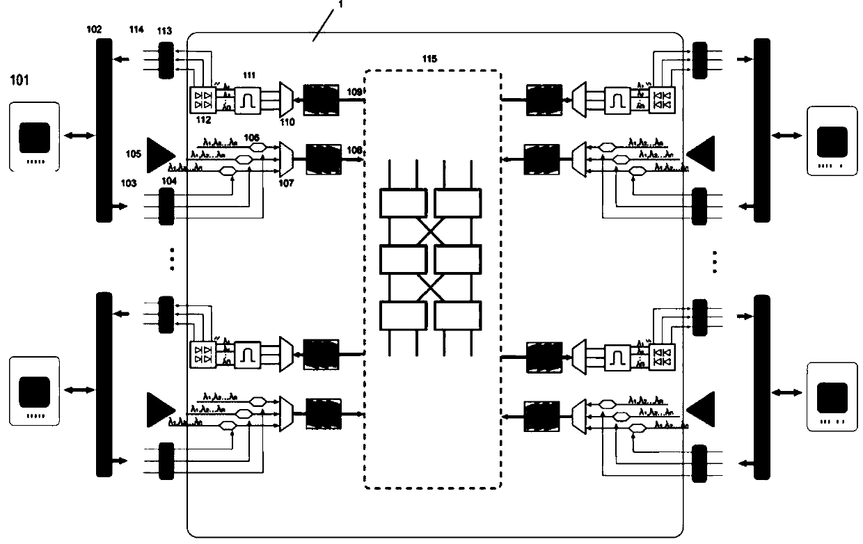
[0028] figure 1 It is a schematic diagram of the overall system architecture of the present invention, which structurally inc...


PUM


Abstract

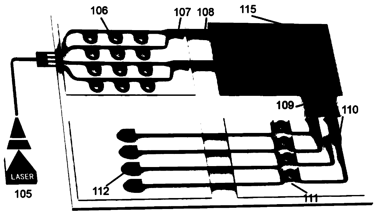
A silicon-based integrated on-chip multimode optical switching system compatible with wavelength division multiplexing signals comprises a multimode optical switching array, N groups of wavelength division-mode division multiplexing optical signal transmitting and receiving systems, and a peripheral driving circuit system, an electrical serial-parallel conversion and parallel-serial conversion system and a high-speed data input and output electrical bus which are used for supporting the system on the chip. According to the system, high-speed serial electric signals generated by data processing nodes are converted into parallel multi-channel electric signals to be input; the optical signal is converted into an optical signal through a modulator array and is loaded on an optical carrier wave of which the wavelength and the mode are multiplexed together; the optical signals enter the multi-mode optical switching array through the multi-mode waveguide input port, are demultiplexed into optical signals of multiple channels after reaching the target port, are converted into parallel electric signals through the photoelectric detector, and are finally reduced into high-speed serial signals to be provided for a data node of the target port for use. The system has the characteristics of low energy consumption, high bandwidth and low delay. The data input interface and the data output interface are both electric domains and are compatible with data interfaces of various existing processors.

Description

technical field [0001] The invention relates to the technical field of on-chip optical interconnection and integrated optics, in particular to a silicon-based integrated on-chip multi-mode optical switching system compatible with wavelength division multiplexing signals. Background technique [0002] In recent years, the method of improving processor performance by increasing the main frequency has encountered the limitation of power consumption. The architecture of multi-core parallel processing has become an important means for continuous improvement of processor performance. The overall performance of a multi-core processor is not only related to the number and performance of the processing cores, but also depends on the communication efficiency between the processing cores. A multi-core processor uses an on-chip network constructed of metal wires to exchange information between processing cores. As more and more processing cores are integrated on a chip, the requiremen...

Claims


Application Information

Patent Timeline
Patent Type & Authority Applications(China)
IPC IPC(8): H04Q11/00G02B6/293
CPCG02B6/2938H04Q11/0005H04Q2011/0007
Inventor 贾浩田永辉杨建红
Owner LANZHOU UNIVERSITY
Learn More