Preparation method of high-sensitivity acceleration sensor structure

An acceleration sensor, high-sensitivity technology, applied in the field of microelectronics, can solve the problems of high cost, inability to accurately and uniformly control the thickness of the cantilever beam, etc., to achieve low cost, eliminate residual stress mismatch, and ensure controllability and uniformity. Effect

Active Publication Date: 2019-07-23
SHANGHAI INST OF MICROSYSTEM & INFORMATION TECH CHINESE ACAD OF SCI
View PDF8 Cites 0 Cited by
  • Summary
  • Abstract
  • Description
  • Claims
  • Application Information

AI Technical Summary

Problems solved by technology

[0005] In view of the shortcomings of the prior art described above, the purpose of the present invention is to provide a method for preparing a high-sensitivity acceleration sensor structure, which is used to solve the problem that the cantilever beam+mass type acceleration cannot be realized on ordinary single crystal silicon wafers in the prior art. The problem of accurate, uniform and controllable thickness of the cantilever beam in the sensor, and the problem of high cost of the controllable thickness of the cantilever beam in the cantilever beam + mass acceleration sensor using SOI silicon chips

Method used


Image

  • Preparation method of high-sensitivity acceleration sensor structure
  • Preparation method of high-sensitivity acceleration sensor structure
  • Preparation method of high-sensitivity acceleration sensor structure

Examples


Embodiment Construction

[0065] Embodiments of the present invention are described below through specific examples, and those skilled in the art can easily understand other advantages and effects of the present invention from the content disclosed in this specification. The present invention can also be implemented or applied through other different specific implementation modes, and various modifications or changes can be made to the details in this specification based on different viewpoints and applications without departing from the spirit of the present invention.

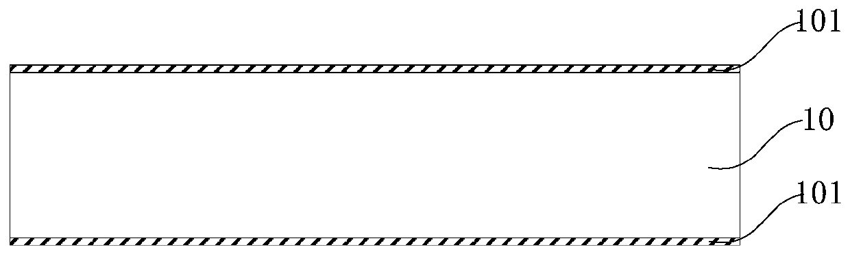
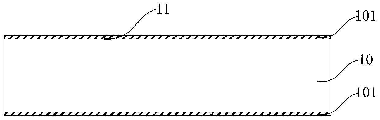
[0066] see Figure 1 to Figure 18 . It should be noted that the diagrams provided in this embodiment are only schematically illustrating the basic concept of the present invention, although only the components related to the present invention are shown in the diagrams rather than the number, shape and Dimensional drawing, the shape, quantity and proportion of each component can be changed arbitrarily during actual implementation, and...


PUM

PropertyMeasurementUnit
widthaaaaaaaaaa
thicknessaaaaaaaaaa
lengthaaaaaaaaaa

Abstract

The invention provides a preparation method of a high-sensitivity acceleration sensor structure. The preparation method comprises the following steps: providing a substrate; performing boron ion implantation on the front surface of the substrate; sequentially forming a first silicon oxide layer and a low-stress silicon nitride layer on the front surface and the back surface of the substrate; forming a release window on the front surface of the substrate; forming a deep groove; forming an internal etching buffer cavity; forming low-stress polycrystalline silicon layers on the side wall of the release window, the side wall of the internal etching buffer cavity and the upper surface and the lower surface of the internal etching buffer cavity; forming a silicon oxide passivation layer on the surface of the low-stress polycrystalline silicon layer; forming a trench on the back surface of the substrate; removing the silicon oxide passivation layer at the bottom of the internal etching buffercavity; preparing a lead hole, a metal lead and a bonding pad on the front surface of the substrate; providing a bonding substrate, and bonding the bonding substrate on the back surface of the substrate; release cantilever beam and mass block. According to the method, the cantilever beam can be prevented from being over-etched, so that the thickness controllability and uniformity of the cantilever beam of any size can be ensured.

Description

technical field [0001] The invention belongs to the technical field of microelectronics, in particular to a preparation method of a high-sensitivity acceleration sensor structure. Background technique [0002] As one of the most popular MEMS detection devices in the field of inertial sensors, silicon-based acceleration sensors are widely used in aerospace, automotive electronics, wearable devices and other consumer electronics products. And with the rise of smart cities, accelerometers will continue to play an increasingly important role. At the same time, with the continuous improvement of MEMS manufacturing technology, the acceleration sensor with high sensitivity, small size and low cost has become the development direction of the acceleration sensor in the future. [0003] As we all know, the sensitivity of the cantilever beam+mass type acceleration sensor is mainly determined by the thickness of the cantilever beam and the size of the mass block. The thinner the cantil...

Claims


Application Information

Patent Timeline
Patent Type & Authority Applications(China)
IPC IPC(8): B81C1/00B81B7/02G01P15/12
CPCB81B7/02B81B2201/0235B81B2203/0118B81C1/0015G01P15/123G01P2015/0862
Inventor 王家畴李昕欣
Owner SHANGHAI INST OF MICROSYSTEM & INFORMATION TECH CHINESE ACAD OF SCI
Why Eureka
Try Eureka