Frequency scanning signal analysis method based on atomic force microscopy technology and application thereof

A technique of atomic force microscopy and frequency signals, applied in special data processing applications, instruments, electrical digital data processing, etc., can solve problems such as relying on experimental test results and unable to analyze

Active Publication Date: 2019-07-23
XIANGTAN UNIV
View PDF3 Cites 0 Cited by
  • Summary
  • Abstract
  • Description
  • Claims
  • Application Information

AI Technical Summary

Problems solved by technology

However, the existing vibration frequency analysis methods for the probe and sample system for AFM technology widely use spring oscillators to replace the interaction between the probe and the sample, which makes the spring oscillator method extremely dependent on experimental test results, and thus cannot analyze specific material properties ( For example: the influence of elastic constant, dielectric constant, piezoelectric coefficient, etc.) on the frequency signal

Method used


Image

  • Frequency scanning signal analysis method based on atomic force microscopy technology and application thereof
  • Frequency scanning signal analysis method based on atomic force microscopy technology and application thereof
  • Frequency scanning signal analysis method based on atomic force microscopy technology and application thereof

Examples


Embodiment 1

[0039] Finite element simulation of probe free resonance frequency:

[0040] (1) Calibration of AFM probe geometry

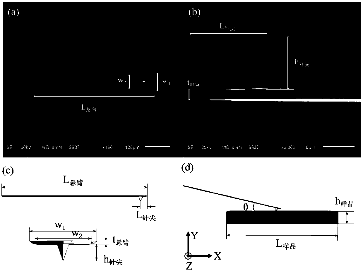
[0041] The AFM probe selects a commercial atomic force microscope conductive probe (model: Econo-SCM-PIC, manufacturer: Asylum Research) made of single crystal silicon, and uses a scanning electron microscope to observe and photograph the morphology of the atomic force microscope conductive probe. figure 2 (a)-(b) are the topography images of the AFM conductive probe observed by the scanning electron microscope, and the geometric dimensions of the probe are calibrated. The main geometric dimensions are: L 针尖 =23.922±1μm, h 针尖 =14.35±1μm, t 悬臂 =2.586±0.2μm, L 悬臂 =480.5±2μm, w 1 =58.33±1μm, w 2 =46.33±1μm, r 针尖 = 20nm.

[0042] (2) Optimization of AFM probe geometry

[0043] Such as figure 2 (c) Establish the finite element model of the probe, and optimize the geometric size of the AFM probe calibrated in step ① as the initial value through the AFM fre...

Embodiment 2

[0050] Probe-piezoelectric sample Pb(Zr 0.2 , Ti 0.8 )O 3 Finite element simulation of the contact resonance frequency of the joint body model.

[0051] figure 2 (d) is the AFM probe and piezoelectric sample Pb(Zr 0.2 , Ti 0.8 )O 3 (hereinafter referred to as PZT) schematic diagram of the contact geometry model. The specific process of the finite element simulation of the free vibration of the AFM probe and the resonant frequency of the AFM probe and the PZT joint model is as follows.

[0052] (1) AFM probe free resonance finite element simulation

[0053] The AFM probe selected here is the same as that in Example 1, and the material parameters of the AFM probe in Example 1 and the optimized probe geometry are adopted.

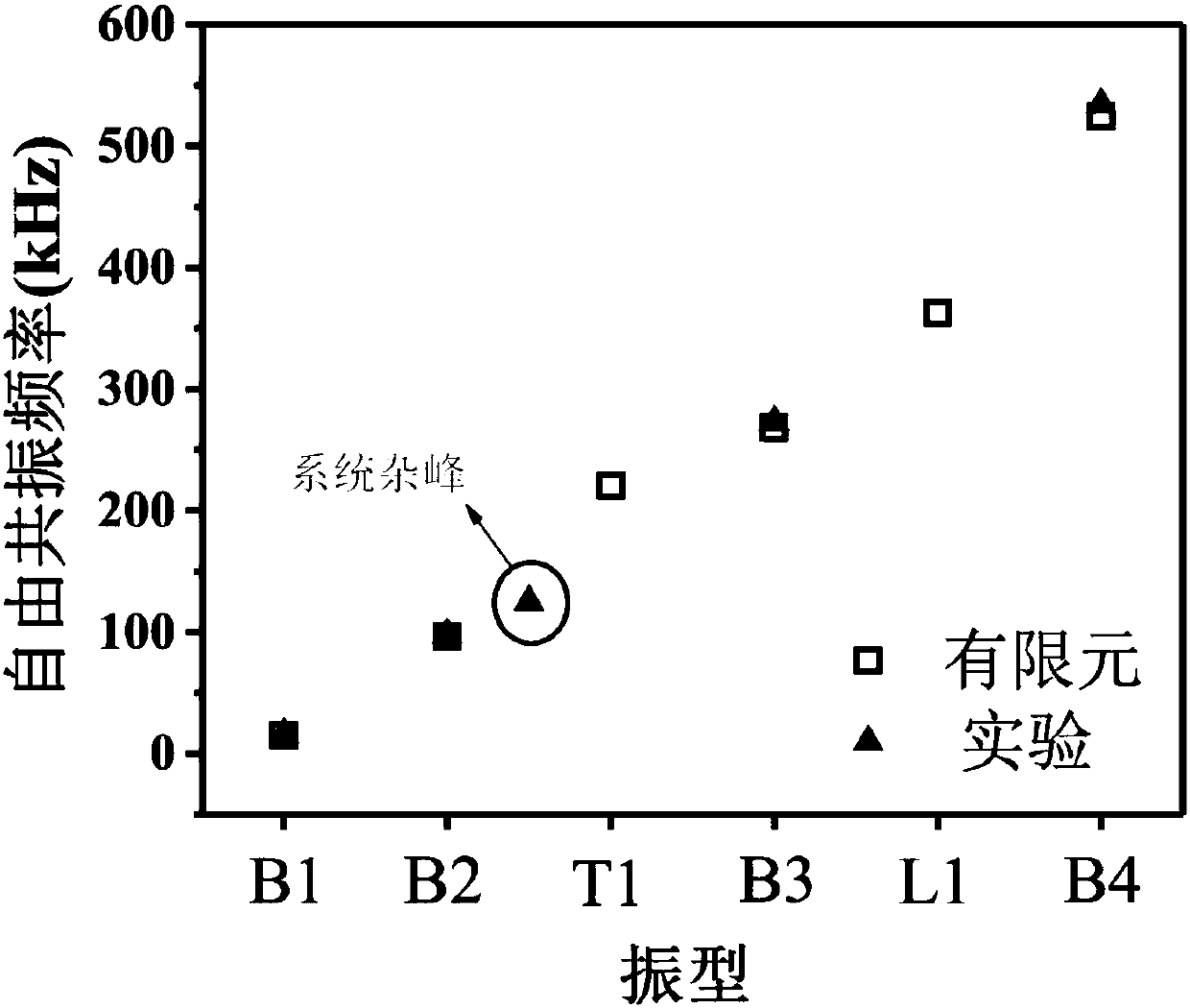
[0054] see image 3 , image 3 It is a comparison chart of the AFM probe free resonance frequency results obtained from the test of the AFM probe under thermal vibration and the finite element calculation. In the thermal vibration test results, B ...

Embodiment 3

[0070] Finite Element Simulation of Contact Resonance Frequency of AFM Probe and Fused Silica Combination Model of Pure Elastic Sample

[0071] (1) Calibration of AFM probe geometry

[0072] The AFM probe is a commercial atomic force microscope conductive probe (model: Nanosensors, NanoWorld Services, Switzerland) made of single crystal silicon, and the morphology of the atomic force microscope conductive probe is observed and photographed by a scanning electron microscope, and the geometry of the probe is Size for calibration: L 悬臂 = 235.2 μm, t = 6.6 μm, h 针尖 = 11.672 μm, w 1 =54.2μm, w 2 = 18.8 μm, r 针尖 = 25nm.

[0073] (2) Setting AFM probe material parameters

[0074] Considering that the material of the selected AFM probe is cubic single crystal silicon, the anisotropy of the elastic properties of the cantilever caused by the different crystal axis orientations of the cubic single crystal silicon makes the cantilever long axis direction, width direction and upper s...


PUM


Abstract

The invention relates to contact resonance frequency signal analysis of an atomic force microscope, in particular to a finite element simulation method for probe-sample contact resonance. The finite element simulation method for probe-sample contact resonance comprises the following steps: establishing a probe free resonance finite element model, and using an experiment free resonance result to fit and optimize the geometric dimension of a probe; establishing probe-sample contact resonance finite element model, determining the inclination angle of the probe, the contact radius and the sample material attribute. According to the contact resonance finite element modeling method, contact resonance frequency signals of different samples and different types of probes are output by taking an atomic force microscope experiment principle as a requirement, high-order contact resonance frequency is calibrated, vibration modes of different-order resonance are judged, and the influence of different material attributes on resonance frequency drift is quantified; powerful discrimination is provided for interference signals, false signals and noise coverage in an AFM experiment; and meanwhile, guidance of probe design is provided for designers.

Description

technical field [0001] The invention relates to frequency signal analysis and application of atomic force microscopy technology, in particular to a contact vibration finite element simulation method of a probe-sample combination and its application. Background technique [0002] Atomic force microscope (AFM) was originally jointly invented by Binning and Quate of the United States and Gerber of Switzerland in 1985. Due to the high resolution imaging capability of AFM, the sample is not limited by conductivity, and can be imaged in various environments, it can not only characterize the surface microscopic morphology of samples, but also characterize the physical properties of materials at the nanometer scale ( Force, electricity, heat, magnetism, light, etc.) and chemical properties, such as surface hardness, surface charge, electric domain and magnetic domain distribution of materials, etc., so AFM is extremely important and widely used in the fields of functional materials,...

Claims


Application Information

Patent Timeline
Patent Type & Authority Applications(China)
IPC IPC(8): G06F17/50
CPCG06F30/23
Inventor 潘锴明文杰山东良刘运牙
Owner XIANGTAN UNIV
Why Eureka
Try Eureka