OSP processing technology for circuit board production
A processing technology and circuit board technology, applied in the directions of printed circuit, printed circuit manufacturing, printed circuit secondary processing, etc., can solve the problems of difficult product quality control, high scrap rate, high production cost, and facilitate the control of processing quality. , The effect of strong biting ability
- Summary
- Abstract
- Description
- Claims
- Application Information
AI Technical Summary
Problems solved by technology
Method used
Image


Examples
Embodiment 1
[0024] Embodiment 1: as figure 1 As shown, the present invention provides a kind of osp processing technique for circuit board production, comprises the steps:
[0025] 1) Feeding: put the PCB board to be processed by OSP on the conveyor belt, and transport the PCB board to each processing station through the conveyor belt;
[0026] 2) Degreasing: a degreasing agent with an acidic concentration of 4% mixed with acetic acid, sulfuric acid, hydrochloric acid and other acids, mainly to remove oxides, SCUM and fingerprints on the surface, and at the same time have an effect on the formed organic protective film Good removal ability, convenient for heavy operation in production;
[0027] 3) Water washing: Spray the above degreased PCB board with a spray pressure of 0.8Kg / cm 2 , and finally wash the PCB board with overflow water, and the overflow flow rate of overflow water washing is 7L / min;
[0028] 4) Micro-etching: Place 3) the PCB board in hydrogen peroxide. The stability of...
experiment example
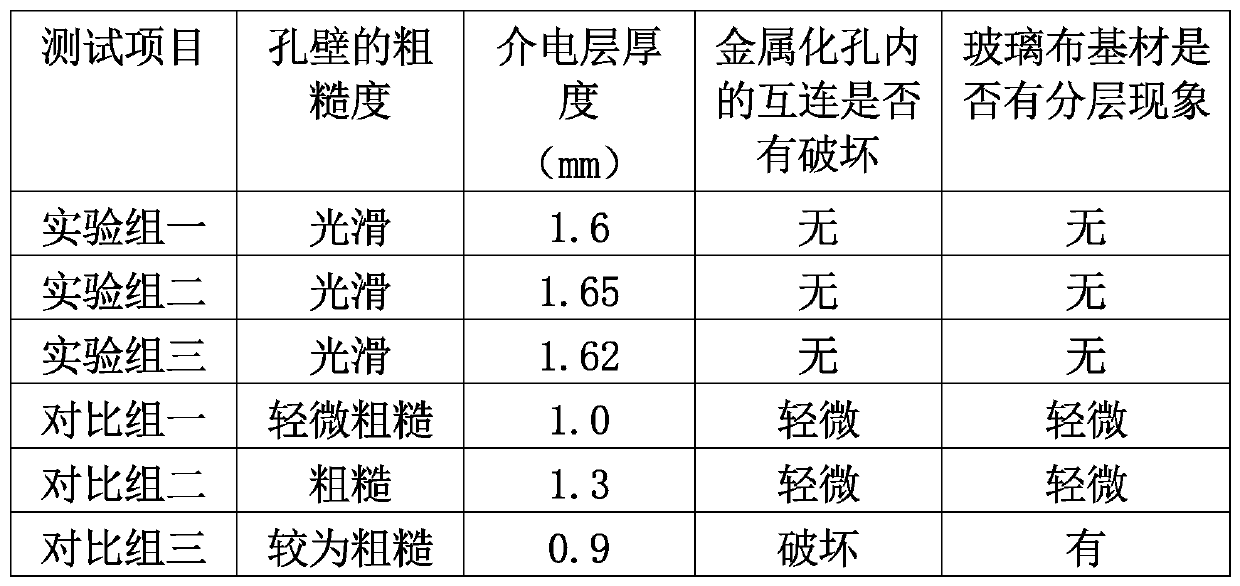
[0046] Experimental object: the circuit boards made by the processing technology of the present invention are used as the experimental group 1, the experimental group 2 and the experimental group 3, and the circuit boards made by other processes on the market are selected as the comparison group 1, the comparison group 2 and the comparison group 3.
[0047] The purpose of the experiment: To test the roughness of the test hole wall of each group of circuit boards, the thickness of the dielectric layer, to observe whether the interconnection in the metallized hole is damaged, and whether there is delamination of the glass cloth substrate.
[0048] Experimental method: Use 600#3M adhesive tape to stick to the green oil surface of the PCB with a length of about 2 inches. Wipe the adhesive surface 3 times with your hands to ensure that it is flat. The adhesive tape can only be used once each time. Pull it up to check whether the tape is attached with solder resist paint, whether the...
PUM
 Abstract
Description
Claims
Application Information
 - R&D
- Intellectual Property
- Life Sciences
- Materials
- Tech Scout
- Unparalleled Data Quality
- Higher Quality Content
- 60% Fewer Hallucinations
Browse by: Latest US Patents, China's latest patents, Technical Efficacy Thesaurus, Application Domain, Technology Topic, Popular Technical Reports.
© 2025 PatSnap. All rights reserved.Legal|Privacy policy|Modern Slavery Act Transparency Statement|Sitemap|About US| Contact US: help@patsnap.com