Preparation method of semiconductor structure

A semiconductor and silicon-on-insulator technology, which is applied in semiconductor/solid-state device manufacturing, semiconductor devices, electric solid-state devices, etc., can solve the problem of uncertain channel current and other problems, and improve the electrical stability of the device and the channel current. Stabilizes and prevents oxidation and wear and tear

Inactive Publication Date: 2019-07-26
SHANGHAI HUALI MICROELECTRONICS CORP
View PDF3 Cites 2 Cited by
  • Summary
  • Abstract
  • Description
  • Claims
  • Application Information

AI Technical Summary

Problems solved by technology

[0004] The purpose of the present invention is to provide a method for preparing a semiconductor structure to solve the problem of uncertain channel current when the existing SONOS flash memory device is turned on

Method used


Image

  • Preparation method of semiconductor structure
  • Preparation method of semiconductor structure
  • Preparation method of semiconductor structure

Examples


preparation example Construction

[0032] The invention provides a method for preparing a semiconductor structure, which includes: providing a semiconductor substrate, an oxide layer is formed on at least a first part of the surface of the semiconductor substrate, and a photoresist layer is formed on at least a second part of the surface; removing a partial thickness of the oxide layer by etching to leave a predetermined thickness of residual oxide layer; and removing the photoresist layer by dry etching.

[0033] Description is made below with reference to the accompanying drawings.

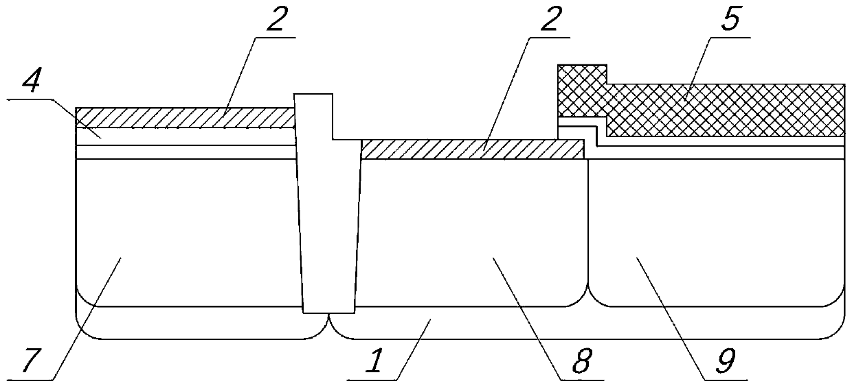
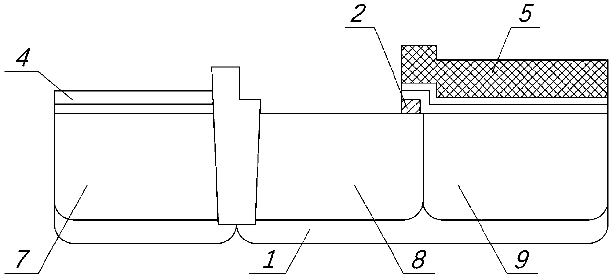
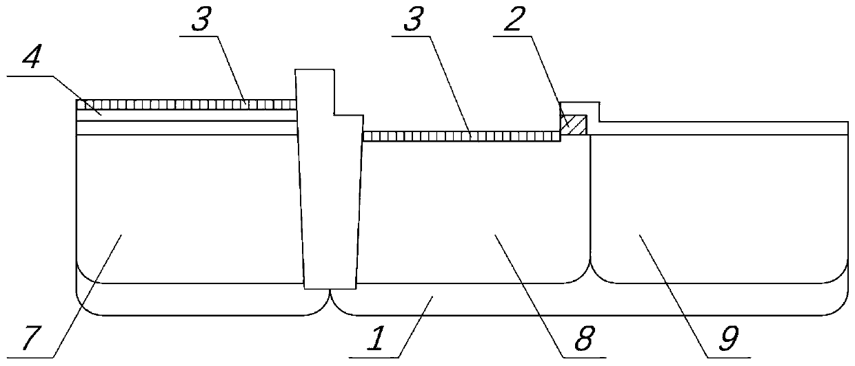
[0034] Please refer to Figure 1 to Figure 3 ,in, figure 1 It is a schematic diagram before wet etching in the process flow of a SONOS flash memory device. figure 2 It is a schematic diagram after wet etching in the process flow of a SONOS flash storage device. image 3 It is a schematic diagram of a SONOS flash storage device process after dry etching and adhesive removal.

[0035] Such as Figure 1 to Figure 3 As shown, t...


PUM


Abstract

The invention provides a preparation method of a semiconductor structure. The preparation method comprises the following steps of providing a semiconductor substrate, wherein an oxide layer is formedon at least a first part of the surface of the semiconductor substrate, and a photoresist layer is formed on at least the second part of the surface; removing the oxide layer with the partial thickness by wet etching so as to retain a residual oxide layer with a preset thickness; and removing the photoresist layer by dry etching. Due to the fact that the residual oxide layer with the preset thickness is still kept in the wet etching process, oxidation and loss of substrate silicon caused by direct exposure of the substrate silicon during dry etching can be prevented. According to the preparation method of the semiconductor structure, the oxide layer with the partial thickness is removed by wet etching, no other process steps need to be added or changed, and the electrical stability of thedevice can be improved on the premise that the cost is not increased.

Description

technical field [0001] The invention relates to the field of semiconductor manufacturing, in particular to a method for preparing a semiconductor structure. Background technique [0002] SONOS flash memory devices have the characteristics of small cell size, low operating voltage, and compatibility with CMOS processes. SONOS flash memory devices use silicon substrate-tunnel oxide layer-silicon nitride-blocking oxide layer (Silicon-Oxide-Nitride) -Oxide-Silicon, SONOS) gate stack replaces the floating gate structure in traditional FLASH memory devices, and is a charge trap type flash memory device. [0003] However, the existing SONOS flash memory device generally has a high-voltage device and a core device, and the high-voltage device and the core device often have the problem of uncertain channel current during conduction, which affects the electrical stability of the device, especially the use of insulators For devices with upper silicon substrates, the thickness of the t...

Claims


Application Information

Patent Timeline
Patent Type & Authority Applications(China)
IPC IPC(8): H01L21/311H01L27/11568
CPCH01L21/31111H10B43/30
Inventor 汪韬辻直樹李妍
Owner SHANGHAI HUALI MICROELECTRONICS CORP
Why Eureka
Try Eureka