Semiconductor device and forming method

A semiconductor and device technology, applied in the field of semiconductor devices and formation, can solve the problems of under-etching at the bottom of through holes, failing to achieve size and shape, affecting device performance, etc., to improve the bottom shape, optimize the filling effect, optimize effect on device performance

Inactive Publication Date: 2019-08-13
SHANGHAI HUAHONG GRACE SEMICON MFG CORP
View PDF4 Cites 2 Cited by
  • Summary
  • Abstract
  • Description
  • Claims
  • Application Information

AI Technical Summary

Problems solved by technology

However, in the etching process of via holes with high aspect ratio, the etching rate will gradually decrease as the depth of the etched via hole increases, which will cause under-etching at the bottom of the via hole or the bottom of the via hole after the etching is completed. The small size does not meet the size and shape required by the design, and it is easy to make it more difficult to fill the conductive material (such as tungsten) in the via hole later, and even cause a hole to be formed under the via hole
In addition, the narrow bottom of the via hole or the void below the via hole will increase the resistance of the semiconductor device and affect the performance of the device.

Method used


Image

  • Semiconductor device and forming method
  • Semiconductor device and forming method
  • Semiconductor device and forming method

Examples


Embodiment Construction

[0031] The specific implementation manner of the present invention will be described in more detail below with reference to schematic diagrams. The advantages and features of the present invention will be more apparent from the following description. It should be noted that all the drawings are in a very simplified form and use imprecise scales, and are only used to facilitate and clearly assist the purpose of illustrating the embodiments of the present invention.

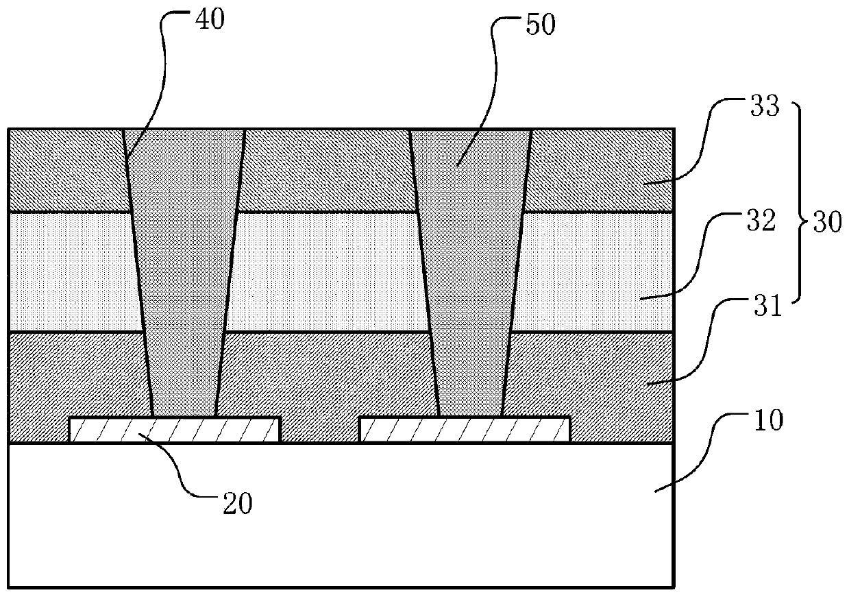
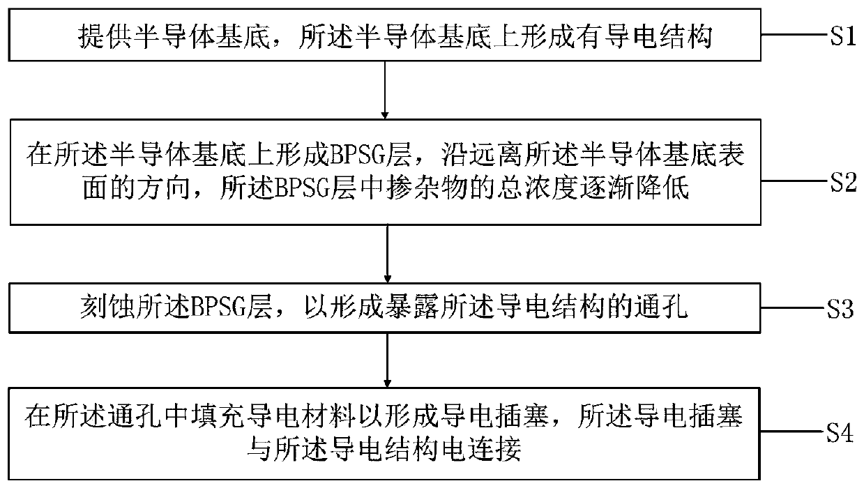
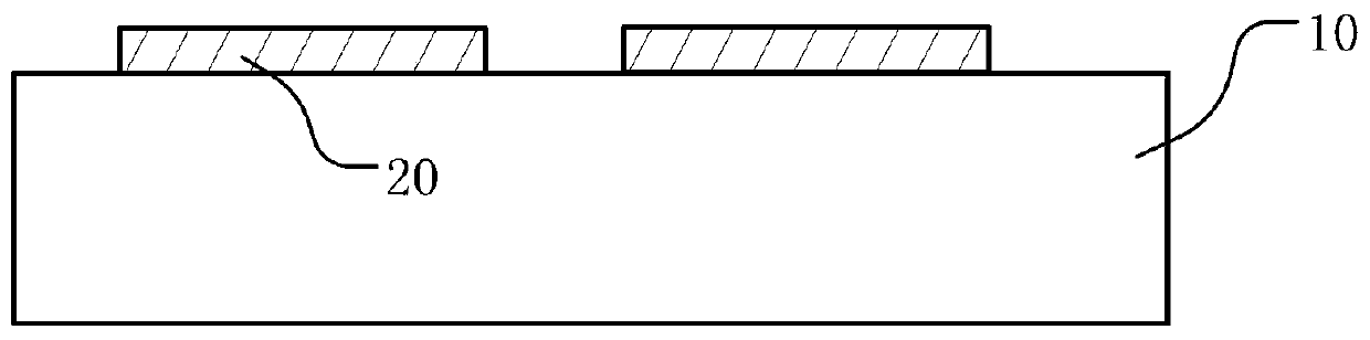
[0032] An embodiment of the present invention provides a semiconductor device. Such as figure 1 As shown, the semiconductor device includes a semiconductor substrate 10 , a dielectric layer 30 and a conductive plug 50 . The conductive structure 20 is formed on the semiconductor substrate 10, the dielectric layer 30 is formed on the semiconductor substrate 10 and covers the surface of the conductive structure 20, and the dielectric layer 30 is also formed with a The layer 30 exposes the through hole 40 of the con...


PUM


Abstract

The invention provides a semiconductor device and a forming method. The semiconductor device comprises a semiconductor substrate, a dielectric layer and a conductive plug, wherein the dielectric layeris located on the semiconductor substrate. The dielectric layer comprises a dopant, and the total doping concentration of the dopant in the dielectric layer is gradually reduced in the direction faraway from the surface of the semiconductor substrate. A through hole for exposing the conductive structure is formed in the dielectric layer, and the conductive plug is disposed in the through hole. The total doping concentration of the dopant in the dielectric layer of the semiconductor device provided by the invention is gradually reduced in the direction far away from the semiconductor substrate; due to the fact that the dielectric layer with the large doping concentration can be etched and removed more easily, when the dielectric layer is etched to form the through hole, the etching rate cannot be obviously reduced along with the increase of the etching depth, the bottom appearance of the through hole can be improved, the through hole meeting the requirement is formed, and then the performance of the semiconductor device is improved.

Description

technical field [0001] The invention relates to the field of semiconductor manufacturing, in particular to a semiconductor device and a forming method. Background technique [0002] Through holes are widely used in semiconductor interconnection technology. At present, in the manufacture of semiconductor devices, the method of forming through holes in the dielectric layer is usually to cover the surface of the dielectric layer with photoresist, and use photolithography to define the through holes. size, and then perform dry etching to finally form a through hole, and further fill the through hole with a conductive material to form a conductive plug. [0003] As the semiconductor process advances to a higher generation, it is necessary to set a via hole with a high aspect ratio (High AspectRatio) in the dielectric layer. A high aspect ratio via hole refers to a ratio of hole depth to hole diameter greater than or equal to 2:1. In this In the structure, borophospho-silicate gl...

Claims


Application Information

Patent Timeline
Patent Type & Authority Applications(China)
IPC IPC(8): H01L23/538H01L21/768
CPCH01L21/76804H01L21/76897H01L23/5384
Inventor 刘冲曹秀
Owner SHANGHAI HUAHONG GRACE SEMICON MFG CORP
Why Eureka
Try Eureka