Super junction device structure and preparation method thereof

A super-junction device and column structure technology, which is applied in the field of super-junction device structure and its preparation, can solve problems such as uneven defects in the super-junction drift region, and achieve the effects of optimizing reverse recovery characteristics, low cost, and increasing recombination probability

Active Publication Date: 2019-08-16
上海功成半导体科技有限公司
View PDF4 Cites 3 Cited by
  • Summary
  • Abstract
  • Description
  • Claims
  • Application Information

AI Technical Summary

Problems solved by technology

[0005] In view of the above-mentioned shortcomings of the prior art, the object of the present invention is to provide a super junction device structure and its preparation method, which is used to solve the problem of uneven introduction of defects in the super junction drift region in the prior art

Method used


Image

  • Super junction device structure and preparation method thereof
  • Super junction device structure and preparation method thereof
  • Super junction device structure and preparation method thereof

Examples


Embodiment 1

[0083] see Figure 1 to Figure 14 , the invention provides a method for preparing a superjunction device structure, comprising the following steps:

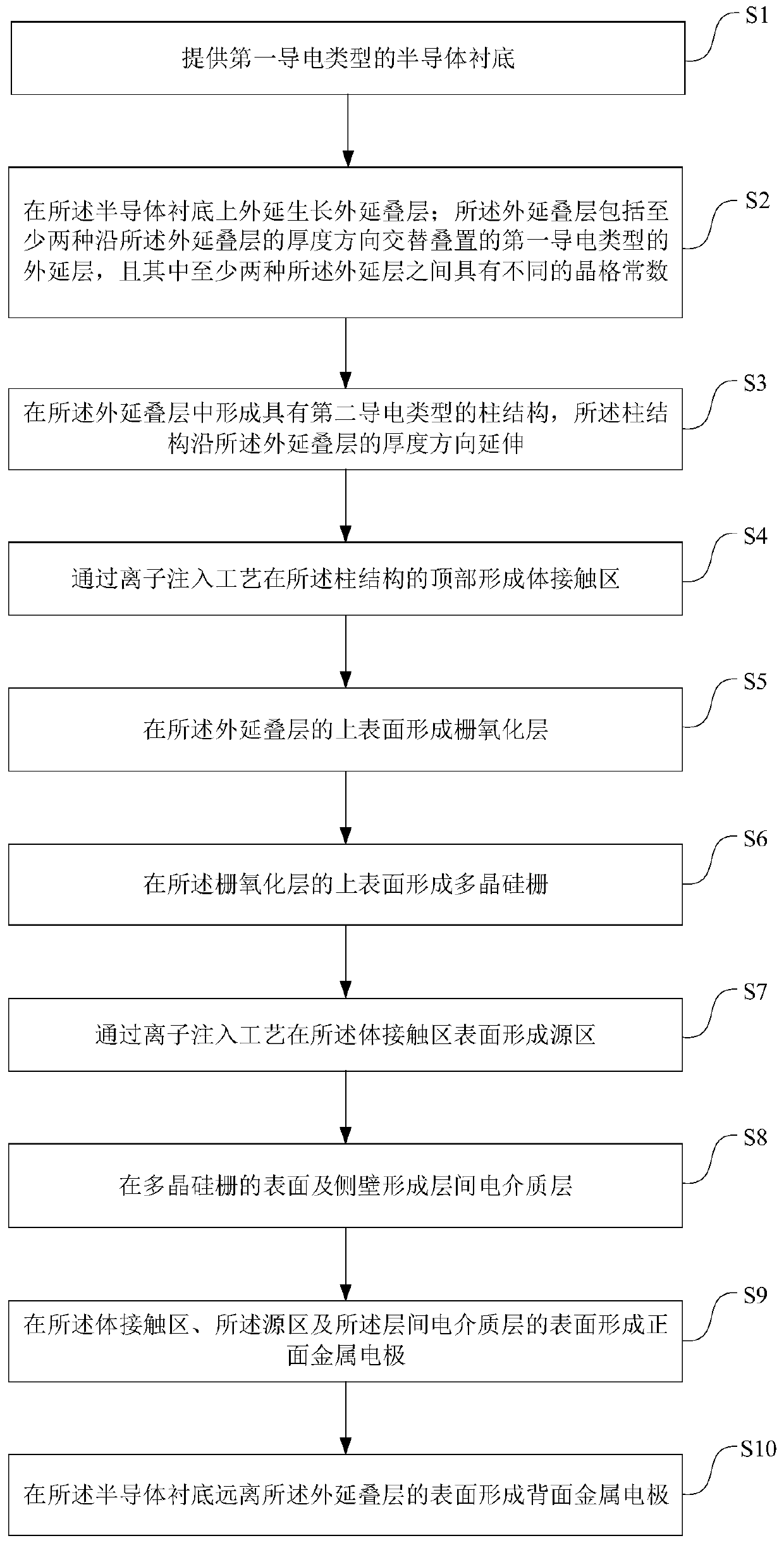
[0084] 1) providing a semiconductor substrate 101 of the first conductivity type;

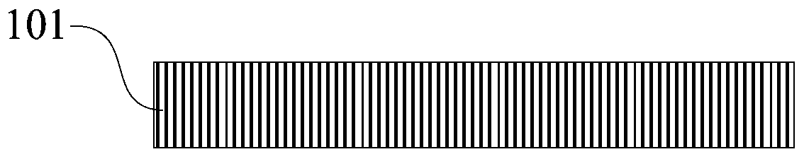
[0085] 2) epitaxially growing an epitaxial stack 102 on the semiconductor substrate 101; the epitaxial stack 102 includes at least two epitaxial layers of the first conductivity type stacked alternately along the thickness direction of the epitaxial stack 102, and wherein at least two of the epitaxial layers have different lattice constants;

[0086] 3) Forming a column structure 103 of the second conductivity type in the epitaxial stack 102 , and the column structure 103 extends along the thickness direction of the epitaxial stack 102 .

[0087] In step 1), see figure 1 The S1 step and figure 2 , providing a semiconductor substrate 101 of the first conductivity type. figure 2 is a schematic cross-sectional view of the semiconductor substra...

Embodiment 2

[0127] Such as Figure 15 As shown, this embodiment provides a super junction device structure and its fabrication method. Compared with Embodiment 1, the difference of this embodiment is that the epitaxial stack 202 on the semiconductor substrate 201 includes three The epitaxial layers of the first conductivity type stacked alternately along the thickness direction of the epitaxial stack 202 specifically include a first epitaxial layer 202a, a second epitaxial layer 202b and a third epitaxial layer 202c.

[0128] As an example, in Figure 15 Among them, the first epitaxial layer 202a and the second epitaxial layer 202b are silicon germanium layers, and the third epitaxial layer 202c is a silicon layer. Wherein, germanium in the first epitaxial layer 202a and the second epitaxial layer 202b have different atomic percentages and percentages. Optionally, the atomic percent content of germanium in the first epitaxial layer 202a is 5%, and the atomic percentage content of german...


PUM


Abstract

The present invention provides a super junction device structure and a preparation method thereof. The super junction device structure includes a semiconductor substrate of a first conductivity type,an epitaxial stack layer formed on the semiconductor substrate, and a column structure of a second conductivity type, wherein the epitaxial stack layer includes at least two epitaxial layers of a first conductivity type alternately stacked along the thickness direction of the epitaxial stack layer, at least one epitaxial layer has a lattice constant different from that of the semiconductor substrate, the column structure is formed in the epitaxial stack layer and extends in the thickness of the epitaxial stack layer. According to the invention, a lattice defect is introduced by growing epitaxial layers of different lattice constants, the carrier recombination probability is increased, and the reverse recovery characteristics of a super junction power device is optimized. Uniformly controllable defect distribution is obtained by introducing the epitaxial stack layer with at least two alternately stacked epitaxial layers. The preparation method provided by the invention has the advantages of simple process and low cost and is suitable for mass production.

Description

technical field [0001] The invention relates to the field of semiconductor integrated circuit manufacturing, in particular to a superjunction device structure and a preparation method thereof. Background technique [0002] In modern life, electric energy is an economical, practical, clean and controllable energy source. For the transmission and conversion of electrical energy, power devices are playing an increasingly important role. Among them, the super junction device (super junction) breaks through the limitation of high withstand voltage and low resistance in traditional silicon-based high-voltage devices, and realizes the device characteristics of high withstand voltage and excellent conduction at the same time, which is a very promising application. power devices. [0003] Currently, the switching speed of super-junction power devices is still very limited. This is due to the unsatisfactory reverse recovery characteristics of the parasitic diode of the super juncti...

Claims


Application Information

Patent Timeline
Patent Type & Authority Applications(China)
IPC IPC(8): H01L29/06H01L29/04H01L29/78H01L21/336
CPCH01L29/0634H01L29/04H01L29/7802H01L29/66712Y02P70/50
Inventor 徐大朋梁欢黄肖艳薛忠营罗杰馨柴展
Owner 上海功成半导体科技有限公司
Why Eureka
Try Eureka