

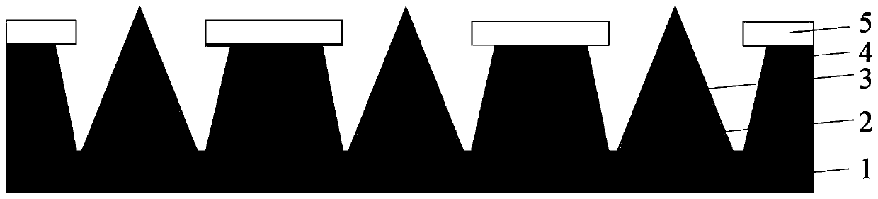
Field emission cathode structure with current limiting resistive switching layer and preparation method thereof
A field emission cathode and resistive layer technology, which is applied in cold cathode manufacturing, electrode system manufacturing, discharge tube/lamp manufacturing, etc., can solve problems such as device damage and cathode gate short circuit, and achieve low manufacturing cost and performance improvement. , the effect of improving launch stability
- Summary
- Abstract
- Description
- Claims
- Application Information
AI Technical Summary
Problems solved by technology
Method used
Image

Examples
Embodiment 1
[0032] This embodiment provides a method for preparing a field emission cathode with a flow-limiting resistive layer, comprising the following steps:
[0033] Step A: Wafer Selection and Cleaning
[0034] In this embodiment, P-type lightly doped silicon wafers are selected, the resistivity is about 3-25Ω / cm-3, and the crystal orientation is 100. Use deionized water, ethanol, acetone, SC-1, SC-2, and deionized water in sequence. ultrasonic cleaning;
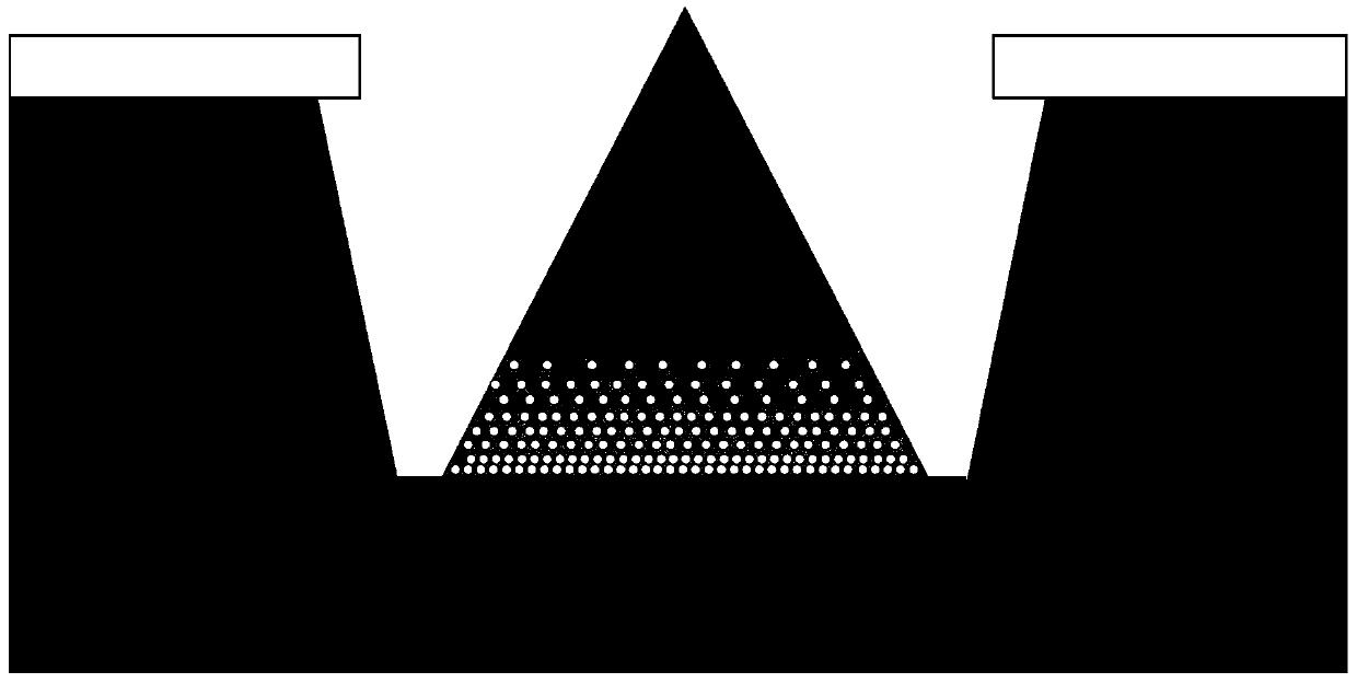
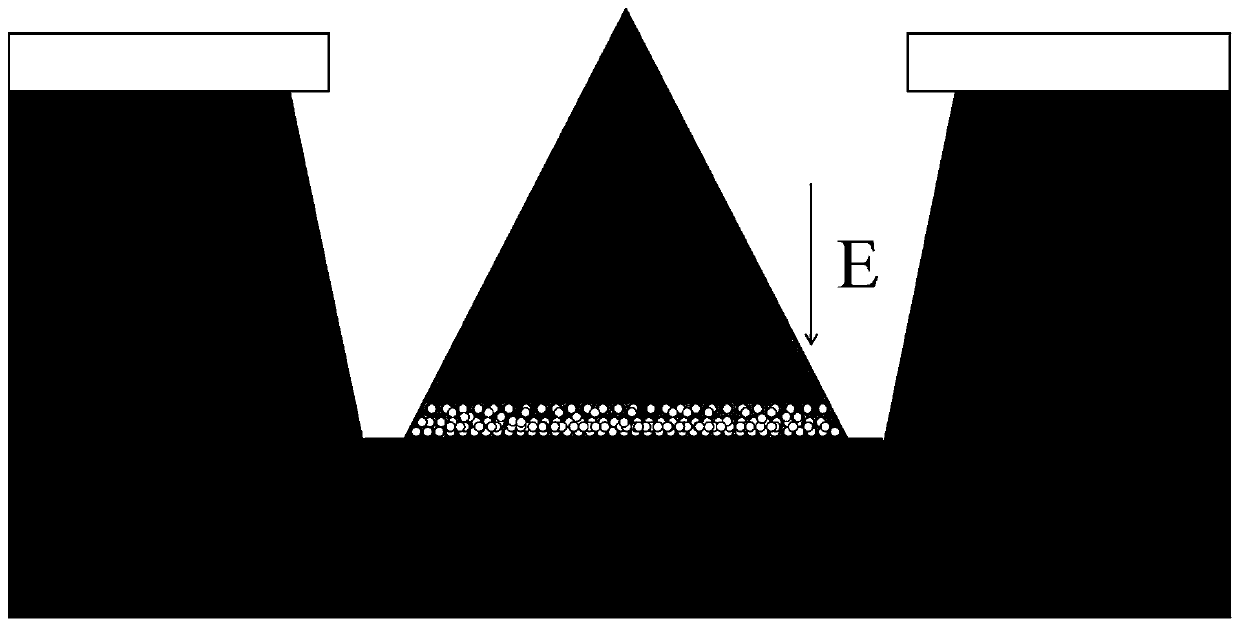
[0035] Step B: Fabrication of Spindt Field Emission Cavity Structure
[0036] The insulating layer is made by the oxidation process, and then the metal gate is made by the sputtering coating process, and then the array pattern is made by the photolithography process and the cavity structure is made by the etching process;
[0037] Step C: Preparing the resistive layer of the metal ion-doped memristive material
[0038] First deposit a silicon oxide layer (SiOx) in the cavity, and then use a sputtering coating process to coat a ...
Embodiment 2
[0045] This embodiment provides a method for preparing a field emission cathode with a flow-limiting resistive layer, comprising the following steps:
[0046] Step A: Wafer Selection and Cleaning
[0047] In this embodiment, P-type lightly doped silicon wafers are selected, the resistivity is about 3-25Ω / cm-3, and the crystal orientation is 100. Use deionized water, ethanol, acetone, SC-1, SC-2, and deionized water in sequence. ultrasonic cleaning;
[0048] Step B: Fabrication of Spindt Field Emission Cavity Structure
[0049] The insulating layer is made by the oxidation process, and then the metal gate is made by the sputtering coating process, and then the array pattern is made by the photolithography process and the cavity structure is made by the etching process;
[0050] Step C: Preparing the resistive layer of the metal ion-doped memristive material
[0051] First deposit a titanium oxide layer (TiOx) in the cavity, and then use a sputtering coating process to coat a...
Embodiment 3
[0057] This embodiment provides a method for preparing a field emission cathode with a flow-limiting resistive layer, comprising the following steps:
[0058] Step A: Wafer Selection and Cleaning
[0059] In this embodiment, P-type lightly doped silicon wafers are selected, the resistivity is about 3-25Ω / cm-3, and the crystal orientation is 100. Use deionized water, ethanol, acetone, SC-1, SC-2, and deionized water in sequence. ultrasonic cleaning;
[0060] Step B: Fabrication of Spindt Field Emission Cavity Structure
[0061] The insulating layer is made by the oxidation process, and then the metal gate is made by the sputtering coating process, and then the array pattern is made by the photolithography process and the cavity structure is made by the etching process;
[0062] Step C: Preparing the resistive layer of the metal ion-doped memristive material
[0063] First, a LaMnO3 layer (LMO) is deposited in the cavity, and then a copper film is deposited on the LaMnO3 laye...
PUM
 Abstract
Description
Claims
Application Information