High-bandwidth GaN-based LED light-emitting device with vertical conductive structure and preparation method thereof

A technology of light-emitting devices and conductive structures, applied in the direction of electric solid devices, semiconductor devices, electrical components, etc., can solve the problems of communication lighting, limited bandwidth of LED devices, insufficient response rate, etc., to reduce the chip contact area and enhance the work. Current density, the effect of reducing difficulty

Inactive Publication Date: 2019-08-30
SOUTH CHINA NORMAL UNIVERSITY
View PDF6 Cites 2 Cited by
  • Summary
  • Abstract
  • Description
  • Claims
  • Application Information

AI Technical Summary

Problems solved by technology

[0003] However, the bandwidth of existing LED devices is limited, the response rate is not enough, and LEDs under high-speed modulation cannot meet the needs of existing communication lighting.

Method used


Image

  • High-bandwidth GaN-based LED light-emitting device with vertical conductive structure and preparation method thereof
  • High-bandwidth GaN-based LED light-emitting device with vertical conductive structure and preparation method thereof
  • High-bandwidth GaN-based LED light-emitting device with vertical conductive structure and preparation method thereof

Examples


Embodiment 1

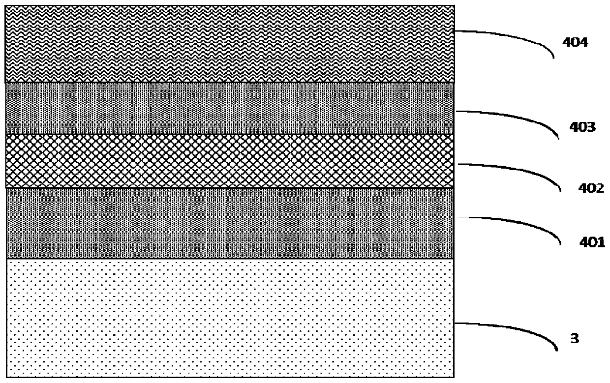
[0030] Such as figure 1 As shown, in this embodiment, MOCVD (metal organic chemical vapor deposition) is used to complete the growth of the LED epitaxial structure 4 on the upper surface of the conductive substrate 3 . The LED epitaxial structure 4 includes, from bottom to top, an N-type doped GaN layer 401 , an InGaN / GaN multi-quantum well active region light-emitting layer 402 , a P-type AlGaN electron blocking layer 403 and a P-type GaN cladding layer 404 .

[0031] The conductive substrate 3 is an m-plane conductive self-supporting GaN homogeneous substrate.

[0032] The N-type doped GaN layer 401 is grown on the upper surface of the conductive substrate 3, and the N-type doping concentration is 1×10 18 cm -3 , the growth temperature is 990°C;

[0033] The InGaN / GaN multi-quantum well active region light-emitting layer 402 is grown on the upper surface of the N-type doped GaN layer 401, by alternately growing InGaN wells and GaN barriers form 5 pairs of multi-quantum w...

Embodiment 2

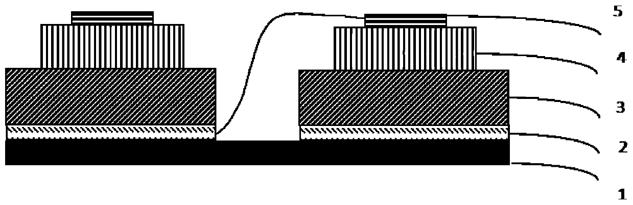
[0047] In this embodiment, the epitaxial growth of the micro-LED with the vertical conductive structure is completed by means of MOCVD. For the epitaxial structure, please refer to figure 1 , the side view of the vertical conductive structure of the LED microarray in series as figure 2 shown. A 3×3 microarray is formed by connecting the N-type electrode and the P-type electrode of a single LED in a head-to-tail series. Its preparation method comprises the following steps:

[0048] 1) Growing an LED epitaxial structure 4 on the upper surface of the conductive substrate 3, the LED epitaxial structure 4 includes an N-type doped GaN layer 401, an InGaN / GaN multi-quantum well active region light-emitting layer 402, and a P-type AlGaN electron blocking layer 403 and a P-type GaN cladding layer 404, the N-type doped GaN layer 401, the InGaN / GaN multiple quantum well active region light-emitting layer 402, the P-type AlGaN electron blocking layer 403 and the P-type GaN cladding la...


PUM


Abstract

The invention discloses a high-bandwidth GaN-based LED light-emitting device with a vertical conductive structure and a preparation method. The light-emitting device is a microarray formed by seriallyconnecting LEDs on an insulating substrate end to end through N-type electrodes and P-type electrodes. Each LED comprises an N-type electrode, a conductive substrate, an LED epitaxial structure and aP-type electrode. The insulating substrate, the N-type electrodes, the conductive substrates, the LED epitaxial structures and the P-type electrodes are sequentially arranged from bottom to top. According to the invention, the micron-sized LEDs are designed to form an array, so that the junction capacitance of the LEDs is reduced, the working current density is increased, and the modulation bandwidth of the LEDs is improved. The current crowding effect of the LEDs is reduced by using the vertical conductive structure, the influence of the heat effect on the bandwidth is reduced, and the modulation bandwidth is further improved.

Description

technical field [0001] The present application relates to the technical field of LED visible light communication, in particular to a high-bandwidth GaN-based vertical conductive structure LED light-emitting device and a preparation method. Background technique [0002] Micro-array LED technology integrates micro-sized LED arrays on a chip with high density through miniaturization and matrixing light-emitting diodes (LEDs), reducing the distance between pixels to the micron level. Its advantages lie in its high photoelectric conversion efficiency, It has the characteristics of high luminous intensity, small size and thinness, and has high response frequency, which can realize the effect of high modulation bandwidth. [0003] However, the bandwidth of the existing LED devices is limited, the response rate is not enough, and the LEDs in the high-speed modulation state cannot meet the needs of the existing communication lighting. The factors that affect the LED modulation chara...

Claims


Application Information

Patent Timeline
Patent Type & Authority Applications(China)
IPC IPC(8): H01L27/15
CPCH01L27/156
Inventor 尹以安王敦年曾妮
Owner SOUTH CHINA NORMAL UNIVERSITY
Why Eureka
Try Eureka