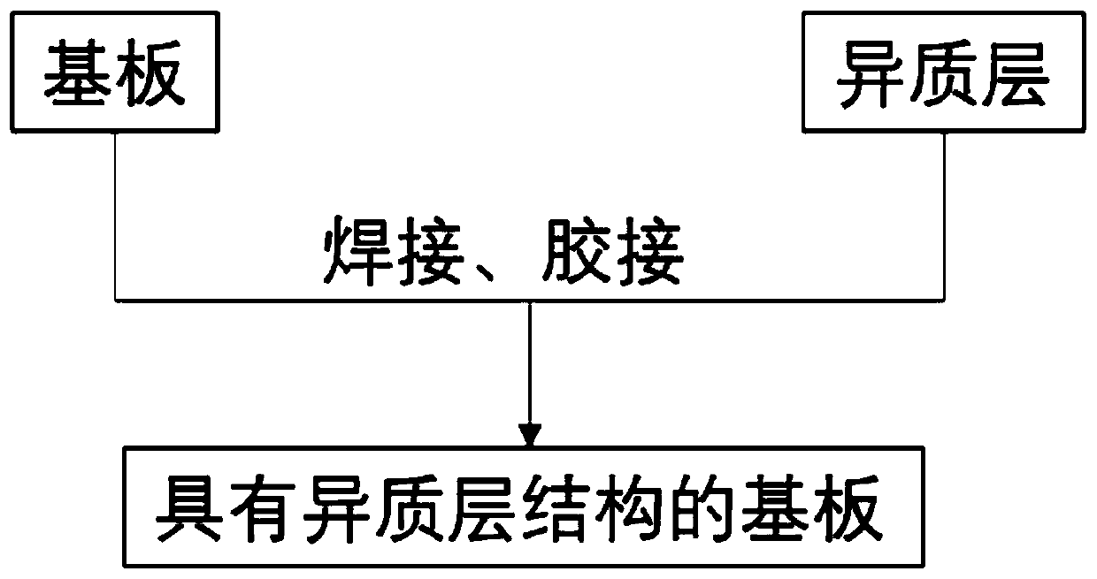
Substrate with heterosphere structure, preparation method and application
A technology of heterogeneous layer and substrate, which is applied in the field of material preparation for microwave devices, can solve the problem that the substrate with heterogeneous layer structure cannot be used in high temperature environment, and achieve the effect of tight combination, high performance reliability, and expanded application
- Summary
- Abstract
- Description
- Claims
- Application Information
AI Technical Summary
Problems solved by technology
Method used
Image


Examples
Embodiment 1
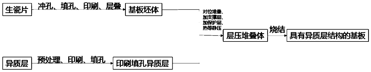
[0056] In this embodiment, a substrate with a heterogeneous layer structure is prepared, and the specific process is as follows:
[0057] (1) Preparation of LTCC substrate green body:
[0058] According to the conventional method, the HL2000 zero-shrinkage green ceramic sheet is sequentially arranged through punching, hole filling, and printing processes to prepare a single-layer LTCC substrate green body, and the substrate green body is laminated, isostatically pressed, and hot-cut to obtain a substrate green body, etc. Static pressure temperature 80℃, pressure 1000PSI, holding time 10min;
[0059] When punching, punch a 0.2mm hole on the substrate as an alignment mark;
[0060] (2) Pretreatment of silicon nitride ceramic thick film plate:
[0061] The heterogeneous layer in this embodiment is a silicon nitride ceramic thick-film plate with a thickness of 0.381mm;
[0062] Firstly, the upper end surface of the silicon nitride ceramic thick film plate is roughened with molt...
Embodiment 2
[0079] In this embodiment, a substrate with a heterogeneous layer structure is prepared, and the specific process is as follows:
[0080] (1) Preparation of LTCC substrate green body:
[0081] According to the conventional method, the HL2000 zero-shrinkage green ceramic sheet is sequentially arranged through punching, hole filling, and printing processes to prepare a single-layer LTCC substrate green body, and the substrate green body is laminated, isostatically pressed, and hot-cut to obtain a substrate green body, etc. Static pressure temperature 80℃, pressure 1000PSI, holding time 10min;
[0082] (2) Pretreatment of barium titanate ceramic thick film plate:
[0083] The heterogeneous layer in this embodiment is a barium titanate ceramic thick-film plate with a thickness of 0.381 mm.
[0084] First, roughen the upper end surface of the barium titanate ceramic thick film plate with molten sodium hydroxide for 50s to obtain a roughened surface, rinse it with deionized water ...
Embodiment 3
[0099] In this embodiment, a substrate with a heterogeneous layer structure is prepared, and the specific process is as follows:
[0100] (1) Preparation of LTCC substrate green body:
[0101] According to the conventional method, the HL800 zero-shrinkage green ceramic sheet is sequentially arranged through punching, hole filling, and printing processes to prepare a single-layer LTCC substrate green body, and the substrate green body is laminated, isostatically pressed, and hot-cut to obtain a substrate green body, etc. Static pressure temperature 80℃, pressure 1000PSI, holding time 10min;
[0102] (2) Pretreatment of tin oxide ceramic thick film board:
[0103] The heterogeneous layer in this embodiment is a tin oxide ceramic thick-film plate with a thickness of 0.481 mm.
[0104] First, roughen the upper end surface of the tin oxide ceramic thick film plate with molten sodium hydroxide for 60 seconds to obtain a roughened surface, rinse it with deionized water and dry it; ...
PUM
| Property | Measurement | Unit |
|---|---|---|
| Thickness | aaaaa | aaaaa |
| Thickness | aaaaa | aaaaa |
| Thickness | aaaaa | aaaaa |
Abstract
Description
Claims
Application Information
 - R&D
- Intellectual Property
- Life Sciences
- Materials
- Tech Scout
- Unparalleled Data Quality
- Higher Quality Content
- 60% Fewer Hallucinations
Browse by: Latest US Patents, China's latest patents, Technical Efficacy Thesaurus, Application Domain, Technology Topic, Popular Technical Reports.
© 2025 PatSnap. All rights reserved.Legal|Privacy policy|Modern Slavery Act Transparency Statement|Sitemap|About US| Contact US: help@patsnap.com