VDMOS device with L-shaped dielectric layer and low EMI

A dielectric layer, L-shaped technology, applied in the electronic field, to achieve the effect of increasing capacitance, simple structure, and reducing circuit volume

Active Publication Date: 2019-09-10
NANJING UNIV OF POSTS & TELECOMM
View PDF3 Cites 6 Cited by
  • Summary
  • Abstract
  • Description
  • Claims
  • Application Information

AI Technical Summary

Problems solved by technology

In the prior art, there is no solution for integrating the RC snubber circuit into the VDMOS device

Method used


Image

  • VDMOS device with L-shaped dielectric layer and low EMI
  • VDMOS device with L-shaped dielectric layer and low EMI
  • VDMOS device with L-shaped dielectric layer and low EMI

Examples


Embodiment Construction

[0025] Below in conjunction with accompanying drawing, technical scheme of the present invention is described in further detail:

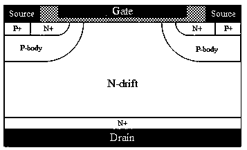
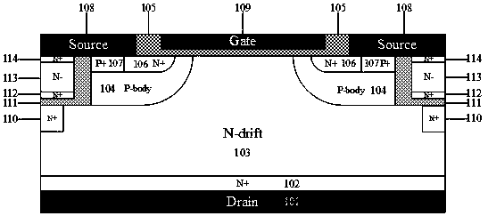
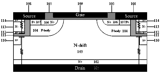
[0026] In the prior art, the VDMOS primary cell structure usually includes a metal electrode 101 at the drain end, an N-type heavily doped active region 102 at the drain end is above the metal electrode 101 at the drain end, and an N-type heavily doped active region 102 at the drain end is above the N-type heavily doped active region 102 at the drain end. Type lightly doped drift region 103, two source well regions 104 are symmetrically distributed on the upper end of the N-type lightly doped drift region, the upper end surface of the drift region is covered with gate silicon dioxide 105, and the entire source well region 104 is P-type light Doping, a fourth N-type heavily doped region 106 and a P-type heavily doped region 107 are arranged above the source well region, part of the region above the source well region 104 is covered with gate silicon ...


PUM


Abstract

The invention provides a VDMOS device with an L-shaped dielectric layer and low EMI. the VDMOS device comprises a VDMOS primitive cell structure, wherein the VDMOS primitive cell structure comprises adrain end metal electrode and a source electrode metal electrode; RC absorption circuits are arranged on the two sides of the VDMOS primitive cell structure, and each RC absorption circuit comprisesa resistor and a capacitor which are connected in series; and one end of the RC absorption circuit is coupled with the source electrode metal electrode, and the other end of the RC absorption circuitis coupled with the drain end metal electrode. On the basis that the original basic electrical property of the VDMOS is ensured, the switching loss and electromagnetic interference of the VDMOS deviceare effectively reduced, and the integration degree of the applied circuit is improved.

Description

technical field [0001] The invention relates to a low-EMI VDMOS device with an L-shaped dielectric layer, in particular to a low-EMI VDMOS device with an internally integrated RC absorbing circuit, and belongs to the field of electronic technology. Background technique [0002] In a switching power supply topology including a transformer, when the switching tube is turned off, the loss caused by the overlap of voltage and current is the main part of the switching power supply loss. At the same time, due to the stray inductance and stray capacitance in the circuit, when the power device is turned off When the overshoot voltage occurs in the circuit and oscillates, it will cause serious electromagnetic interference (EMI, Electromagnetic Interference) to the outside. If the spike voltage is too high, it will damage the power device. At the same time, the existence of oscillation will also increase the output ripple. In order to reduce the turn-off loss and peak voltage, it is...

Claims


Application Information

Patent Timeline
Patent Type & Authority Applications(China)
IPC IPC(8): H01L29/78H01L23/552
CPCH01L29/7802H01L29/7803H01L23/552
Inventor 王玲成建兵沈醴田莉陈明
Owner NANJING UNIV OF POSTS & TELECOMM
Why Eureka
Try Eureka