Double-gate vacuum field emission triode structure and preparation method thereof

A field emission and triode technology, applied in the direction of electrical components, circuits, semiconductor devices, etc., can solve the problems of high vacuum degree requirements, complex preparation process, unfavorable circuit integration and other problems, achieve good electron emission performance, simple preparation process, Effect of Good Electron Transport Properties

Active Publication Date: 2019-09-17
XI AN JIAOTONG UNIV
View PDF3 Cites 1 Cited by
  • Summary
  • Abstract
  • Description
  • Claims
  • Application Information

AI Technical Summary

Problems solved by technology

[0004] Researchers at home and abroad have carried out a lot of experimental research on the device materials, structural design and preparation process of VFET, but the preparation process is often complicated or not conducive to circuit integration, and the device requires a high degree of vacuum in the working environment
Canon Corporation of Japan proposed a "electrical formation" process when researching Surface-conduction Electron-emitter Display (SED), which can crack the film to obtain narrower cracks through the Joule heat generated by electrification. , but not applied in VFET studies

Method used


Image

  • Double-gate vacuum field emission triode structure and preparation method thereof
  • Double-gate vacuum field emission triode structure and preparation method thereof
  • Double-gate vacuum field emission triode structure and preparation method thereof

Examples


Embodiment 1

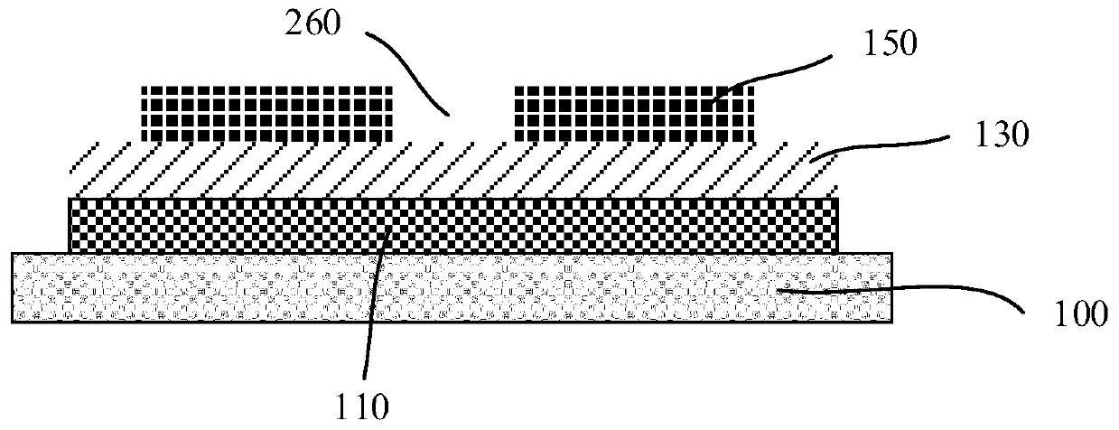
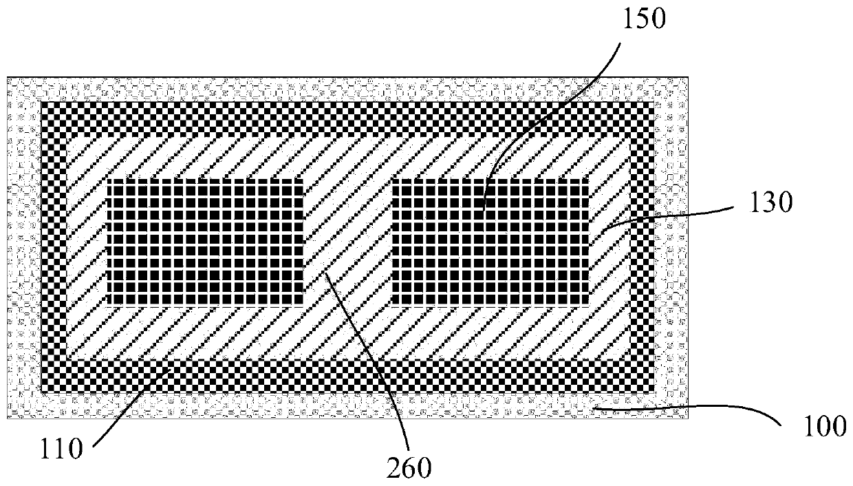
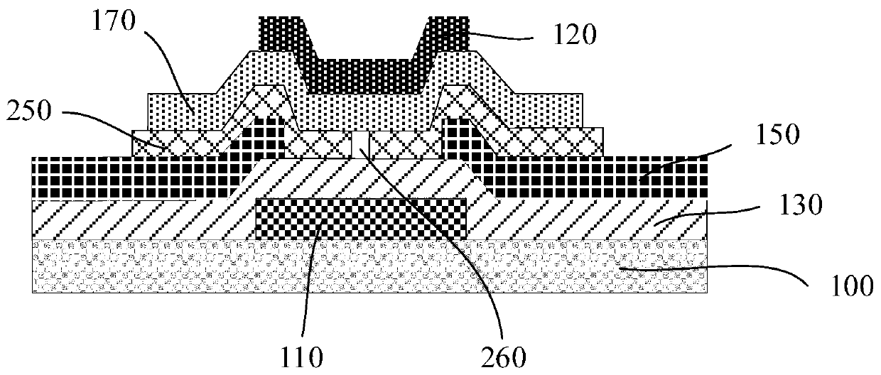
[0061] A double-gate vacuum field emission transistor structure, including a bottom gate 110 deposited on a substrate 100, a bottom gate insulating layer 130 is deposited on the bottom gate 110, and a symmetrical source is deposited on the bottom gate insulating layer 130. The drain electrode 150 has a conductive film 250 deposited on the source-drain electrode 150, a top gate insulating layer 170 is deposited on the conductive film 250, and a top gate 120 is deposited on the top gate insulating layer; between the symmetrical source-drain electrodes 150 An electrode gap of 5-15 μm is provided between them; a nanoscale vacuum channel 260 is provided in the middle of the conductive film 250 .

[0062] The thickness of the bottom gate 110 is 50-200nm; and the bottom gate 110 is made of one or more materials among nickel, copper, platinum, silver, chromium and molybdenum.

[0063] The bottom gate insulating layer 130 has a thickness of 50-250 nm; and the bottom gate insulating lay...

Embodiment 2

[0072] see image 3 with Figure 4 , is a schematic diagram of a double-gate VFET device structure disclosed in the present invention, including a bottom gate 110, a bottom gate insulating layer 130, a source-drain electrode 150, a conductive film 250, a top gate insulating layer 170, a top gate 120 and a vacuum channel 260 .

[0073] The fabrication process of the structure, the specific steps are as follows:

[0074] 1) Fabricate the bottom grid 110 on the substrate 100 by magnetron sputtering or electron beam evaporation, the bottom grid has a thickness of 50-200 nm, a length of 300-500 μm, and a width of 20-50 μm;

[0075] 2) Fabricate the bottom gate insulating layer 130 on the bottom gate 110 by chemical vapor deposition or magnetron sputtering, and the thickness of the bottom gate insulating layer is 50-250nm;

[0076] 3) Fabricate symmetrical source-drain electrodes 150 on the bottom gate insulating layer 130 by magnetron sputtering or electron beam evaporation. Th...


PUM


Abstract

The invention discloses a double-gate vacuum field emission triode structure and a preparation method thereof, and belongs to the field of information technology and the field of vacuum microelectronic devices. The triode structure includes a bottom gate, a bottom gate insulating layer, source and drain electrodes, a conductive film, a top gate insulating layer, a top gate, and a nano-scale vacuum channel. The double-gate vacuum field emission triode can realize the double-gate control of a device current, enhances the gate voltage control capability and the modulation flexibility of the device, and achieve good electron emission performance. The top of the vacuum channel is covered with the top gate insulating layer and the top gate such that the collision scattering effect of atmospheric particles on electrons is reduced during electron transport. Thus, the device can work directly in the atmospheric environment and has good electron transport performance. The vacuum channel prepared by the method has a nano-scale size and good uniformity, and contributes to the large-scale and low-cost preparation of the device.

Description

technical field [0001] The invention belongs to the field of information technology and the field of vacuum microelectronic devices, and relates to a structure of a double-gate vacuum field emission transistor and a manufacturing method thereof, in particular to a double-gate modulation capability and a relatively low requirement on the vacuum degree of the working environment or can be used. The structure and manufacturing method of a vacuum field emission triode working in an atmospheric environment. Background technique [0002] The vacuum field emission triode (Vacuum Field Emission Triode, VFET) prepared by Gray of the U.S. Naval Laboratory based on the field electron emission array of silicon material is a vacuum microelectronic device, which has the advantages of both solid-state electronic devices and vacuum electronic devices. . [0003] Unlike traditional vacuum tubes that use hot cathodes as the electron emission source, VFETs use field emission cold cathodes as ...

Claims


Application Information

Patent Timeline
Patent Type & Authority Applications(China)
IPC IPC(8): H01L29/06H01L29/10H01L29/78
CPCH01L29/0684H01L29/1033H01L29/78
Inventor 吴胜利龙铭刚张劲涛刘逸为
Owner XI AN JIAOTONG UNIV
Why Eureka
Try Eureka