A kind of phononic crystal and thin-film piezoelectric acoustic wave sensor
A piezoelectric acoustic wave and phononic crystal technology, applied in the field of sensors, can solve the problems of limited energy and the inability to effectively improve the quality factor of thin-film piezoelectric acoustic wave sensors, and achieve high quality factor, limited energy dissipation, and efficient reflection.
- Summary
- Abstract
- Description
- Claims
- Application Information
AI Technical Summary
Problems solved by technology
Method used
Image
Examples
Embodiment 1
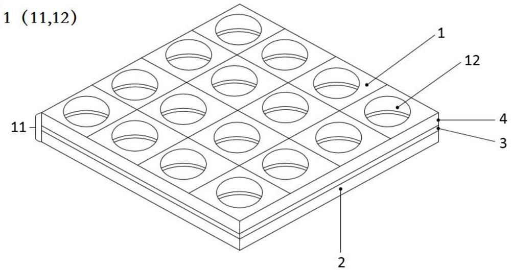
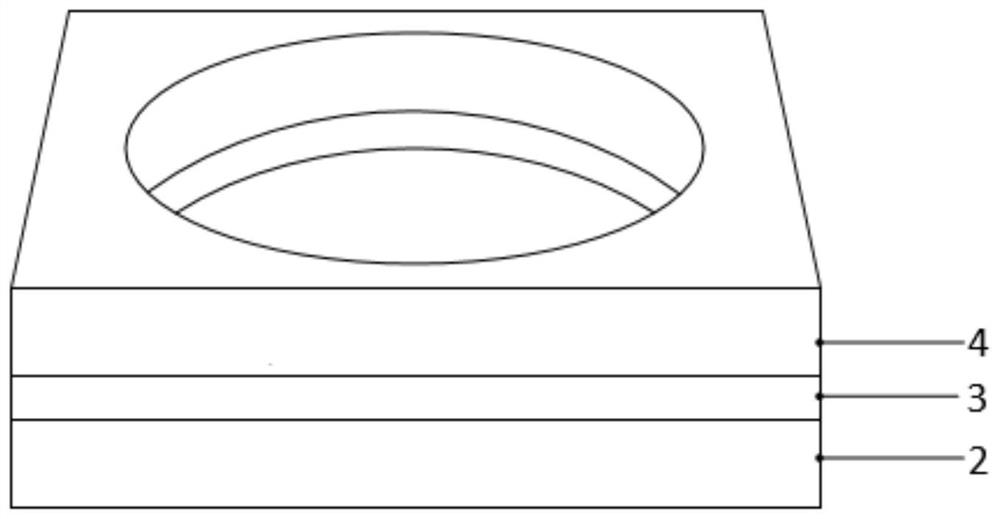
[0053] This embodiment provides a phononic crystal 1 . The phononic crystal 1 is composed of a base 11 and a scatterer 12 formed on the base 11 . like figure 1 and figure 2 As shown, the matrix 11 of the phononic crystal 1 is a composite dielectric layer formed by sequentially stacking three dielectric layers of the piezoelectric layer 4, the ground electrode layer 3 and the substrate layer 2; The periodically arranged through holes form the scatterer 12 of the phononic crystal 1 .
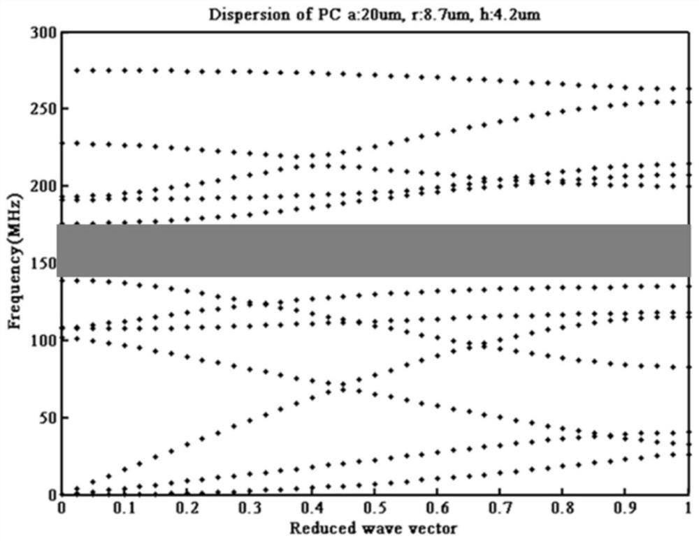
[0054] Specifically, such as figure 2 In the shown unit cell phononic crystal 1, the through hole is a cylindrical hole that runs through the composite phononic crystal 1, figure 2 The smallest periodic structural unit of phononic crystal 1 is shown in . The single-cell phononic crystals 1 are arranged in a square lattice, forming as figure 1 The shown phononic crystal 1 has through-holes arranged periodically, wherein the through-holes extend along the length and width directions of the p...
Embodiment 2
[0072] This embodiment provides a thin film piezoelectric acoustic wave sensor, such as Figure 11 As shown, it includes a substrate layer 2 , a ground electrode layer 3 and a piezoelectric layer 4 stacked in sequence, and at least one interdigital transducer 5 is provided on the side of the piezoelectric layer 4 away from the ground electrode layer 3 . For example, the thin-film piezoelectric acoustic wave sensor is a two-port type, and the side of the piezoelectric layer 4 away from the ground electrode layer 3 is horizontally oppositely provided with two transducers 5 , namely an input transducer and an output transducer. The transducer 5 is specifically an interdigital transducer 5, and the input transducer and the output transducer correspond to the input interdigital transducer and the output interdigital transducer respectively. The two sides of the transducer 5 are respectively provided with phononic crystals 1, that is, on the side where the input IDT is facing away f...
experiment example 1
[0085] This experimental example tests the phononic crystal 1 formed on the aluminum nitride layer, molybdenum layer and silicon substrate layer in the thin-film piezoelectric acoustic wave sensor of Example 2, and the phononic crystal 1 formed only on the silicon substrate layer in the thin-film piezoelectric acoustic wave sensor of Comparative Example 1 The phononic crystal 1, the improvement effect of the acoustic wave transmission loss in the thin film piezoelectric sensor, is as follows:
[0086] 1. Adjust the filling rate of the phononic crystal 1 (that is, the area of the cylindrical through hole / the area of the square lattice), and detect the change of the bandgap width of the phononic crystal 1 in the thin-film piezoelectric acoustic wave sensor. The results are as follows Figure 13 as shown, Figure 13 middle f 1 represents the lower edge frequency of the band gap of phononic crystal 1, f 2 Represents the upper edge frequency of the bandgap of phononic crystal...
PUM
 Abstract
Description
Claims
Application Information


