Method for measuring thickness of nanoscale film by utilizing photon spin Hall effect

A technology of spin Hall effect and thin film thickness, applied in the optical field, can solve the problems of low system assembly accuracy, difficult to popularize and apply on a large scale, low accuracy of turntable, etc., meet the requirements of low instrument requirements, suitable for large-scale application, high precision The effect of measurement

Active Publication Date: 2019-09-27
ZHENGZHOU UNIVERSITY OF LIGHT INDUSTRY
View PDF5 Cites 5 Cited by
  • Summary
  • Abstract
  • Description
  • Claims
  • Application Information

AI Technical Summary

Problems solved by technology

In this measurement method, if the precision of the turntable is low, or the assembly precision of the system is low, it is difficult to ensure that the spot position of the reflected beam at the image processing unit is constant when PSHE does not occur
If the position of the spot moves at this time, the amount of movement will be directly superimposed on the measured spin-splitting displacement, resulting in measurement error, which in turn will cause a decrease in measurement accuracy
In this invention, if you want to ensure that the spot position of the reflected beam at the image processing unit is constant during the change of the incident angle (assuming that PSHE does not occur), you need to use a high-precision turntable to strictly ensure the accuracy of the assembly , and to ensure the vibration of the measurement environment and other factors, which will inevitably lead to an increase in the cost of the measurement system, so the inventive method is not easy to apply on a large scale

Method used


Image

  • Method for measuring thickness of nanoscale film by utilizing photon spin Hall effect
  • Method for measuring thickness of nanoscale film by utilizing photon spin Hall effect
  • Method for measuring thickness of nanoscale film by utilizing photon spin Hall effect

Examples


Embodiment Construction

[0039] The technical solutions of the present invention will be clearly and completely described below in conjunction with the embodiments of the present invention. Obviously, the described embodiments are only some of the embodiments of the present invention, not all of them. Based on the embodiments of the present invention, all other embodiments obtained by persons of ordinary skill in the art without making creative efforts belong to the protection scope of the present invention.

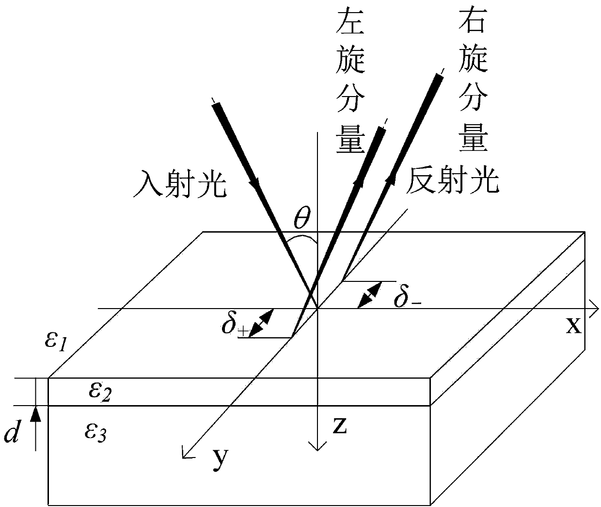
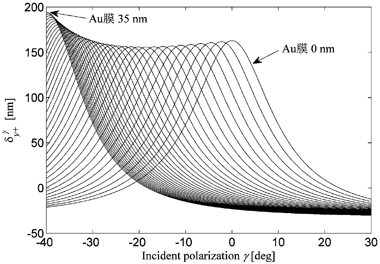
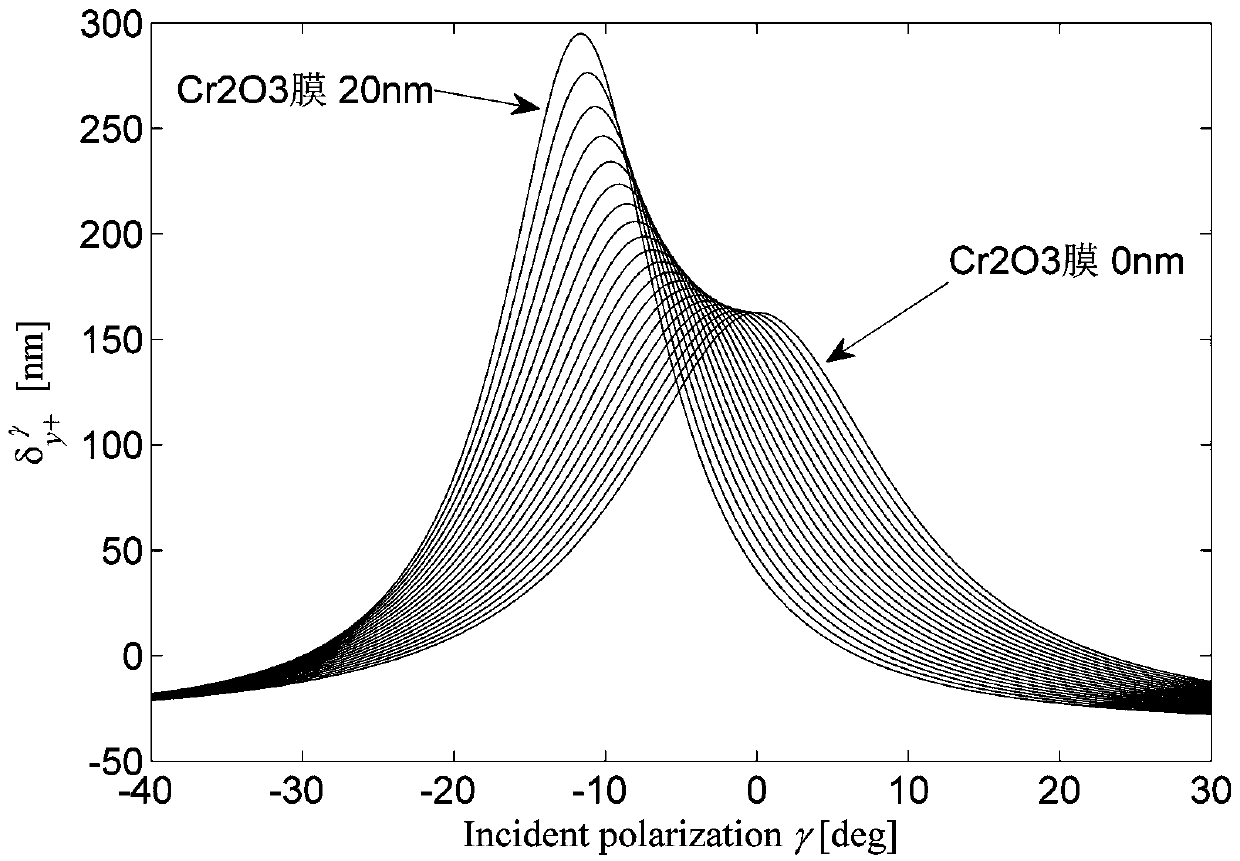
[0040] A method to measure the thickness of nanoscale films by using the photon spin Hall effect, and then to measure the metal material gold Au and the non-metal material chromium trioxide Cr 2 o 3 film thickness as an example, refer to Figure 10 The step flow chart describes in detail the specific implementation process of the present invention.

[0041] The incident light beam that adopts in the embodiment of the present invention is that wavelength is 632.8nm, beam waist w 0 Gaussian bea...


PUM


Abstract

The invention belongs to the field of optics, and relates to a method for measuring the thickness of a nanoscale film, in particular to a method for measuring the thickness of the nanoscale film by utilizing a photon spin Hall effect. The method comprises the following steps: establishing a theoretical database in which PSHE splitting displacement changes along with incident polarization states under different materials and different film thicknesses; selecting a group of incident polarization, enabling incident light to be incident to the surface of a measured film at a certain initial incident polarization, and obtaining spin splitting displacement under the incident polarization; sequentially changing a polarization angle of the incident light to obtain measurement data of spin splitting displacement along with the changes of the incident polarization angle; and calculating and comparing the obtained measurement data with theoretical data under each film thickness, and determining the thickness of the measured film. According to the invention, the dependence relationship between the spin splitting displacement of PSHE under different incident polarization and the film thickness is utilized to realize non-contact, lossless and high-precision measurement of the metal and non-metal material film thickness, and the measurement system is simple in structure and convenient to operate.

Description

technical field [0001] The invention belongs to the field of optics, and relates to a method for measuring the thickness of a nanoscale film, in particular to a method for measuring the thickness of a nanoscale film by using the photon spin Hall effect. Background technique [0002] With the wide application of thin film technology in the fields of microelectronics, optoelectronics, aerospace, bioengineering, weaponry, food science, medical equipment and polymer materials, thin film technology has become a research hotspot in the field of current scientific and technological research and industrial production. Especially the rapid development of thin film technology has directly affected the development direction of science and technology and people's way of life. The continuous improvement and rapid development of thin-film manufacturing technology also put forward higher requirements for various parameters of the thin film, such as the thickness and refractive index parame...

Claims


Application Information

Patent Timeline
Patent Type & Authority Applications(China)
IPC IPC(8): G01B11/06
CPCG01B11/06
Inventor 秦自瑞姜利英任林娇张培姜素霞张吉涛王延峰
Owner ZHENGZHOU UNIVERSITY OF LIGHT INDUSTRY
Why Eureka
Try Eureka