Connecting material for being connected with silicon carbide material and application of connecting material

A technology for connecting materials and silicon carbide, applied in the composite field, can solve problems such as difficulty in meeting actual use requirements, and achieve the effect of achieving local seamless connection, similar macro performance, and promoting connection and densification.

Active Publication Date: 2019-10-15
NINGBO INST OF MATERIALS TECH & ENG CHINESE ACADEMY OF SCI
View PDF3 Cites 4 Cited by
  • Summary
  • Abstract
  • Description
  • Claims
  • Application Information

AI Technical Summary

Problems solved by technology

However, it is still difficult to meet the practical needs

Method used


Image

  • Connecting material for being connected with silicon carbide material and application of connecting material
  • Connecting material for being connected with silicon carbide material and application of connecting material
  • Connecting material for being connected with silicon carbide material and application of connecting material

Examples


Embodiment 1

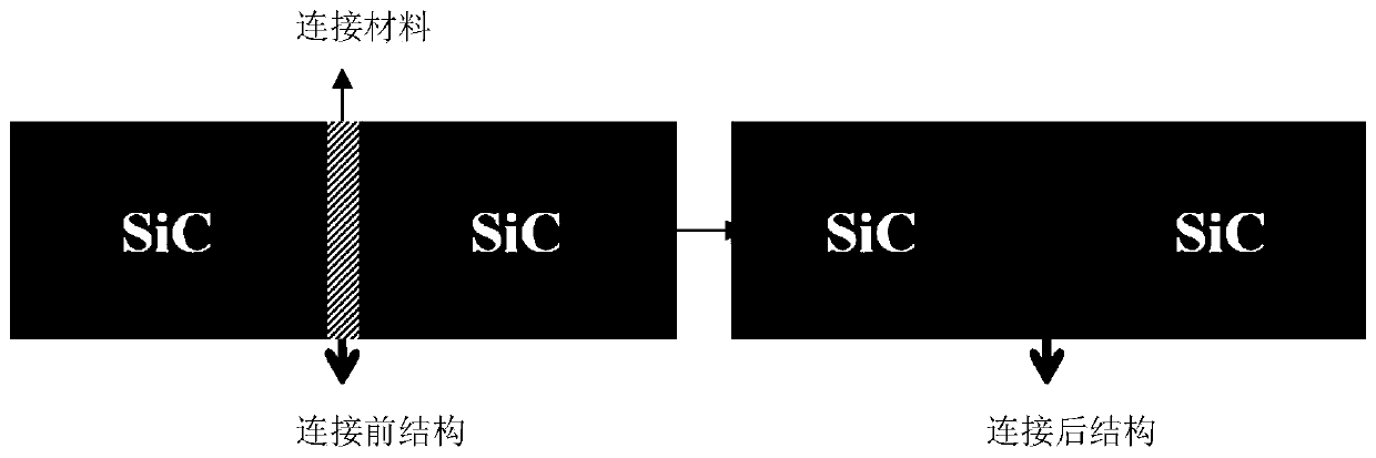
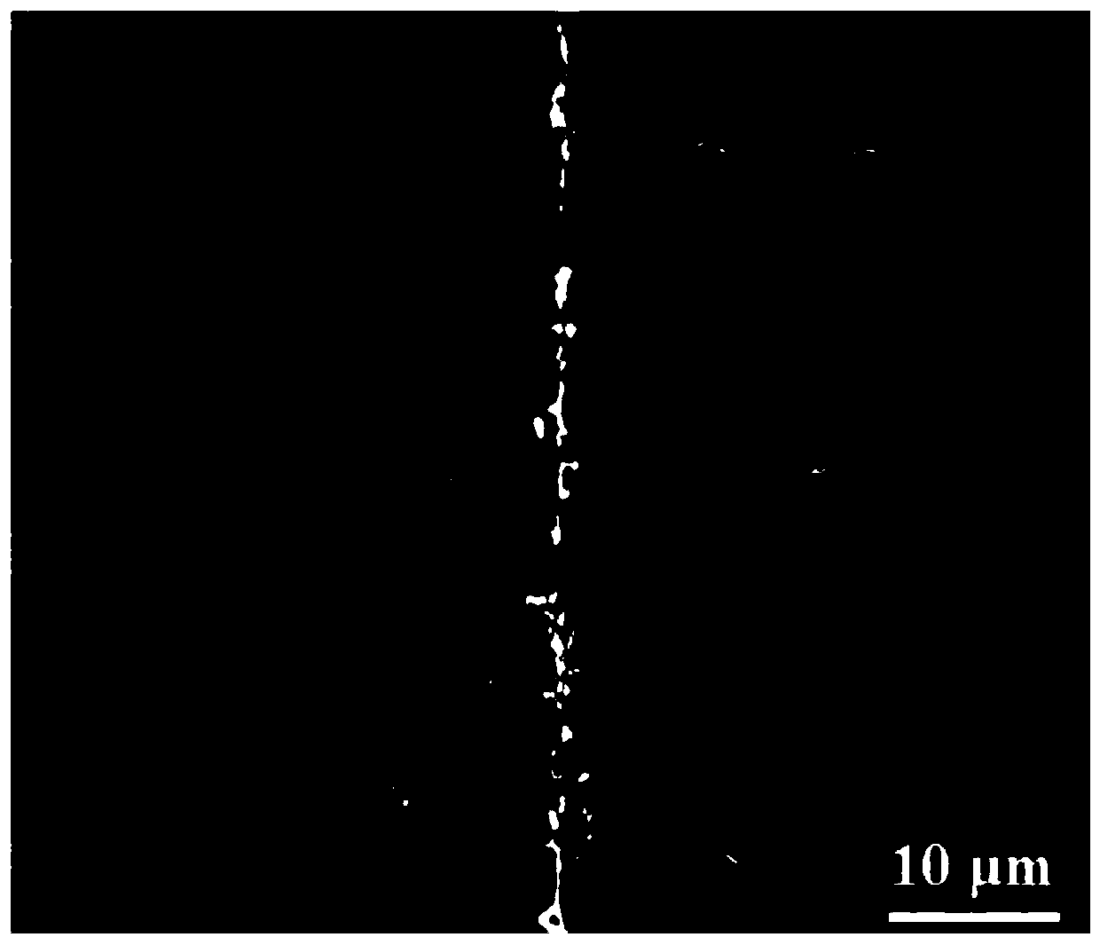
[0063] In this example, if figure 1 Shown is a schematic diagram of the connection structure of 500 nm Er-bonded SiC ceramics. The material to be connected is two Ф20×20mm silicon carbide, the material of the connection layer is 500nm Er, and the connection interface is assisted by electric field heating to make the connection interface reach 1900°C, so as to connect the SiC materials to be connected together. Specific steps are as follows:

[0064] (1) Polish the surface of silicon carbide to be connected to 1 μm with diamond polishing liquid to remove surface defects and impurities;

[0065] (2) Coating a 500nm Er film on the surface of a piece of silicon carbide to be connected by physical vapor deposition, and then connecting another piece of silicon carbide to its surface; then put the sample into a graphite mold, and then place the graphite mold in a spark plasma sintering furnace In the process, current is applied, and the temperature is raised to 1900°C at a heating ...

Embodiment 2

[0069] In this example, if figure 1 Shown is a schematic diagram of the connection structure of 500nm Dy-bonded SiC ceramics. The material to be connected is two Ф30×30mm silicon carbide, and the material of the connection layer is a 500nm Dy film. The connection interface is assisted by electric field heating to make the connection interface reach 1900°C, thereby connecting the SiC materials to be connected together. Specific steps are as follows:

[0070] (1) Polish the surface of silicon carbide to be connected to 1 μm with diamond polishing liquid to remove surface defects and impurities;

[0071] (2) Use physical vapor deposition to coat a 500nm Dy film on the surface of a silicon carbide to be connected, and then connect another silicon carbide to its surface; then put the sample into a graphite mold, and then place the graphite mold in a spark plasma sintering furnace During the heating process, the current is applied, and the temperature is raised to the furnace temp...

Embodiment 3

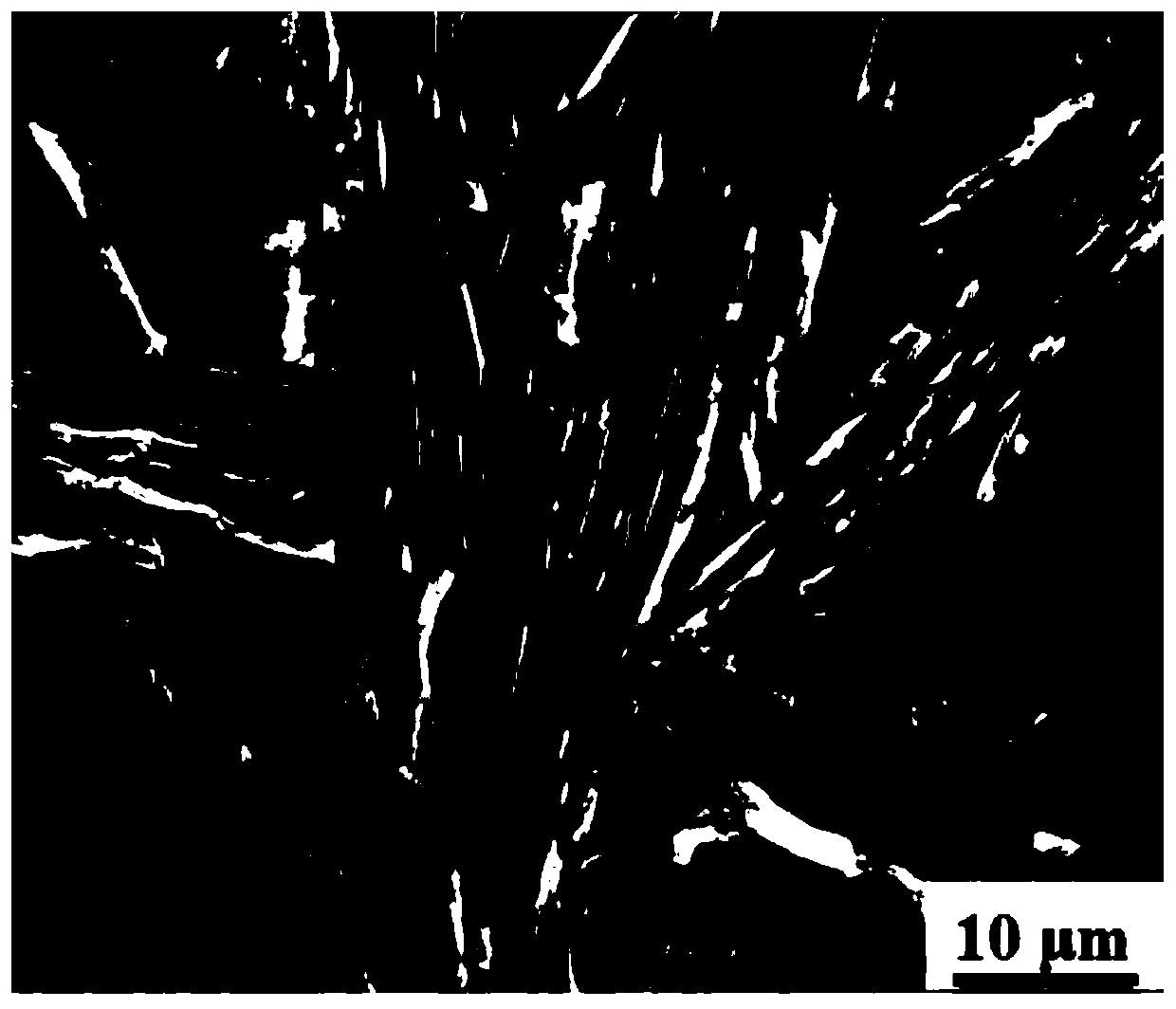
[0075] In this example, if figure 1 Shown is a schematic diagram of the connection structure of 500nm Er-coated SiC composite material connected to SiC ceramics. The materials to be connected are two Ф20×20mm silicon carbide, and the connection layer material is 500nm Er-coated silicon carbide composite material. The connection interface is assisted by electric field heating to make the connection interface reach 1600°C, so that the SiC materials to be connected are connected together . Specific steps are as follows:

[0076] (1) Polish the surface of silicon carbide to be connected to 1 μm with diamond polishing liquid to remove surface defects and impurities;

[0077] (2) Prepare 500nm Er-coated silicon carbide composite material by molten salt method, and make a casting film, sandwich the 500nm Er-coated silicon carbide composite material casting film between two pieces of silicon carbide, and then place the sample Put the graphite mold into the graphite mold, then place...


PUM

PropertyMeasurementUnit
thicknessaaaaaaaaaa
thicknessaaaaaaaaaa
bending strengthaaaaaaaaaa

Abstract

The invention discloses a connecting material for being connected with a silicon carbide material and an application of the connecting material. The connecting material comprises any one or combination of two or more of lanthanide rare earth element, ternary layered rare earth silicide and a lanthanide rare earth element coated silicon carbide composite, wherein the chemical formula of ternary layered rare earth silicide is Re3Si2C2, and Re represents the lanthanide rare earth element. The invention further discloses the application of the lanthanide rare earth element, ternary layered rare earth silicide or the lanthanide rare earth element coated silicon carbide composite to connection with the silicon carbide material, and also discloses a connecting method of the silicon carbide material. The characteristic of high-temperature instability of layered rare earth silicide is utilized, and generation of a rare earth liquid phase facilitates densified sintering of joint interface silicon carbide; the obtained silicon carbide connecting structure is high in bending strength and excellent in high-temperature resistance, oxidization resistance and corrosion resistance and can be applied to extreme service environments such as aerospace, nuclear systems and the like.

Description

technical field [0001] The invention relates to the technical field of connection of silicon carbide ceramics and composite materials thereof, in particular to a lanthanide rare earth element Re and a ternary layered rare earth carbon silicide Re 3 Si 2 C 2 1. The lanthanide rare earth element Re coats the silicon carbide composite material to connect the connection material of the silicon carbide material, and its application in the connection layer of the silicon carbide and its composite material, which can be used in the technical field of silicon carbide and its composite material connection. Background technique [0002] Silicon carbide (Silicon carbide, SiC) has excellent high-temperature mechanical properties, as well as good oxidation resistance, corrosion resistance, and radiation resistance. Silicon carbide and its composite materials (including silicon carbide ceramics, silicon carbide ceramic matrix composites, such as Silicon carbide fiber reinforced silicon ...

Claims


Application Information

Patent Timeline
Patent Type & Authority Applications(China)
IPC IPC(8): C04B37/00
CPCC04B37/003C04B35/64C04B2237/12C04B2237/365C04B2237/52C04B2237/36C04B2235/666
Inventor 周小兵刘俊文邹顺睿黄政仁黄庆
Owner NINGBO INST OF MATERIALS TECH & ENG CHINESE ACADEMY OF SCI
Why Eureka
Try Eureka