

Preparation method of selenium selenide thin film with certain forbidden band width
A germanium selenide and band gap technology, which is applied in semiconductor/solid-state device manufacturing, photovoltaic power generation, electrical components and other directions, can solve the problems of complex process, high cost, and many amorphous germanium selenide, etc., and achieves the preparation process. Simple, fast heating rate and short reaction period
- Summary
- Abstract
- Description
- Claims
- Application Information
AI Technical Summary
Problems solved by technology
Method used
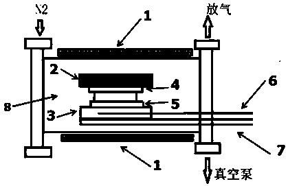
Image

Examples
Embodiment Construction
[0043] Below in conjunction with specific embodiment, further illustrate the present invention. It should be understood that these examples are only used to illustrate the present invention and are not intended to limit the scope of the present invention. In addition, it should be understood that after reading the contents of the present invention, those skilled in the art may make various changes or modifications to the present invention, and these equivalent forms also fall within the scope of the present invention.
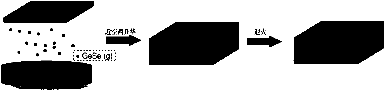
[0044]The preparation of germanium selenide thin films with different band gaps by the present invention is divided into two steps, comprising preparation of amorphous germanium selenide thin films by near-space sublimation and annealing of amorphous germanium selenide thin films, such as figure 1 shown.
PUM
 Abstract
Description
Claims
Application Information