Method for producing semiconductor device

A manufacturing method and semiconductor technology, applied in semiconductor/solid-state device manufacturing, electrical components, circuits, etc., can solve problems such as reducing the controllability of aluminum diffusion to semiconductor substrates, and achieve the effect of improving controllability

Active Publication Date: 2019-10-18
SHINDENGEN ELECTRIC MFG CO LTD
View PDF7 Cites 0 Cited by
  • Summary
  • Abstract
  • Description
  • Claims
  • Application Information

AI Technical Summary

Problems solved by technology

[0007] That is to say, there are following problems in the manufacturing method of semiconductor device in the past: Namely, the dielectric type i

Method used


Image

  • Method for producing semiconductor device
  • Method for producing semiconductor device
  • Method for producing semiconductor device

Examples


Embodiment 1

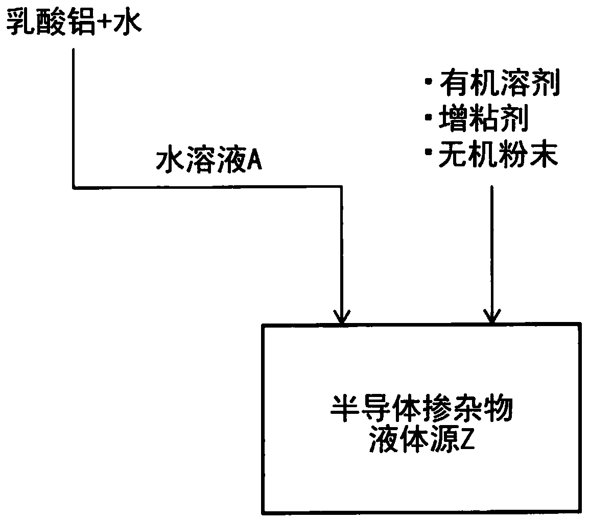
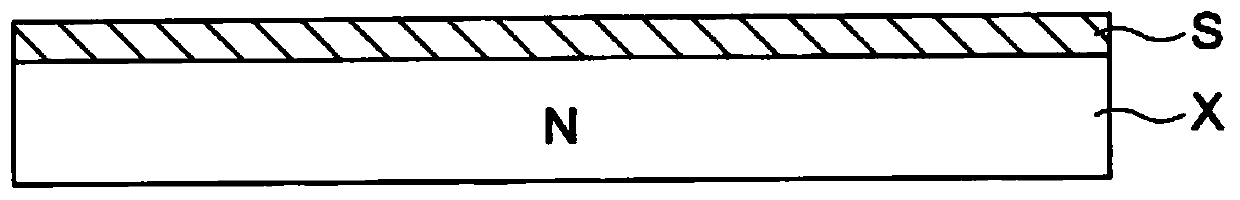
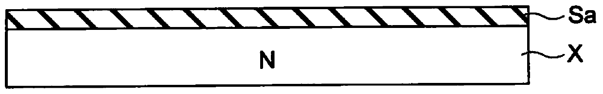
[0075] figure 1 It is a diagram showing a configuration example of a semiconductor dopant liquid source in the method for manufacturing a semiconductor device of the present invention. Figure 2 to Figure 5 It is a process illustration diagram of the manufacturing method of the semiconductor device concerning Example 1.

[0076] The manufacturing method of the semiconductor device related to the first embodiment is as follows Figure 2 to Figure 5 As shown, the "dissolving step", "mixing step", "coating step", "firing step", "diffusion step", and "peeling step" were sequentially carried out. Next, the method of manufacturing the semiconductor device according to the first embodiment will be described in the order of the above-mentioned steps.

[0077] Dissolving process

[0078] First, aluminum lactate was dissolved in water to make aqueous solution A ( figure 1 ).

[0079] Here, as the liquid source of the P-type semiconductor dopant for diffusing the P-type dopant on ...

Embodiment 2

[0121] In one of the above-mentioned embodiments, a mode in which aluminum as a P-type dopant is diffused on one semiconductor substrate has been described. However, as described above, aluminum as a P-type dopant can be diffused on a plurality of (two or more) semiconductor substrates by laminating semiconductor substrates.

[0122] In the second embodiment, a mode in which a desired dopant is diffused on a plurality of semiconductor substrates by stacking semiconductor substrates will be described in detail. In the second embodiment, the diffusion process in the first embodiment is described as a deposition process and a diffusion process.

[0123] (Semiconductor dopant liquid source)

[0124] First, the semiconductor dopant liquid source related to the second embodiment will be described.

[0125] The semiconductor dopant liquid source according to the second embodiment is heated while being applied between a plurality of stacked semiconductor substrates, so that dopants ...


PUM


Abstract

This method for producing a semiconductor device comprises: a dissolving step wherein aluminum lactate is dissolved in water, thereby preparing an aqueous solution; a mixing step wherein a mixed liquid is prepared by mixing the aqueous solution and an organic solvent with each other, and a semiconductor impurity liquid source that contains the mixed liquid is prepared; a coating step wherein the semiconductor impurity liquid source that contains the aqueous solution is applied onto a semiconductor substrate after the mixing step, thereby forming a diffusion source coating film on the semiconductor substrate; a firing step wherein the semiconductor substrate is subjected to a heat treatment at a first temperature in a first atmosphere after the coating step, thereby firing at least the organic solvent in the diffusion source coating film; and a diffusing step wherein the semiconductor substrate is subjected to a heat treatment at a second temperature that is higher than the first temperature in a second atmosphere after the firing step, thereby having the aluminum, which is contained in the diffusion source coating film, diffused into the semiconductor substrate so as to form a diffusion layer in the semiconductor substrate.

Description

technical field [0001] The present invention relates to a method of manufacturing a semiconductor device. Background technique [0002] Conventionally, there has been a method of manufacturing a conductor device in which a diffusion source covering film containing an aluminum compound and a boron compound is formed as a P-type dopant on a semiconductor substrate, and by heating the semiconductor substrate on which the diffusion source covering film is formed, Thereby, a P-type diffusion layer was formed on the semiconductor substrate (see Japanese Unexamined Patent Publication No. 2000-286205). [0003] In particular, in order to obtain a P-type low-concentration and deep diffusion layer, it is necessary to use aluminum with a large diffusion coefficient. [0004] As the manufacturing method of the above-mentioned conventional semiconductor device, there can be exemplified: the method of dissolving aluminum compound and boron compound in a solvent and coating on the wafer (...

Claims


Application Information

Patent Timeline
IPC IPC(8): H01L21/225
CPCH01L21/225H01L21/228
Inventor 小笠原淳六鎗广野
Owner SHINDENGEN ELECTRIC MFG CO LTD
Why Eureka
Try Eureka