Electronic assembly welding spot for temperature circulation
An electronic component and temperature cycle technology, applied in the direction of electrical components, electrical solid devices, circuits, etc., can solve the problems of increasing the cost of electronic components, long filling process, and increasing manufacturing time, so as to reduce the occurrence probability of solder joint fracture and relieve Stress, the effect that is conducive to miniaturization
- Summary
- Abstract
- Description
- Claims
- Application Information
AI Technical Summary
Problems solved by technology
Method used
Image

Examples
Embodiment 1
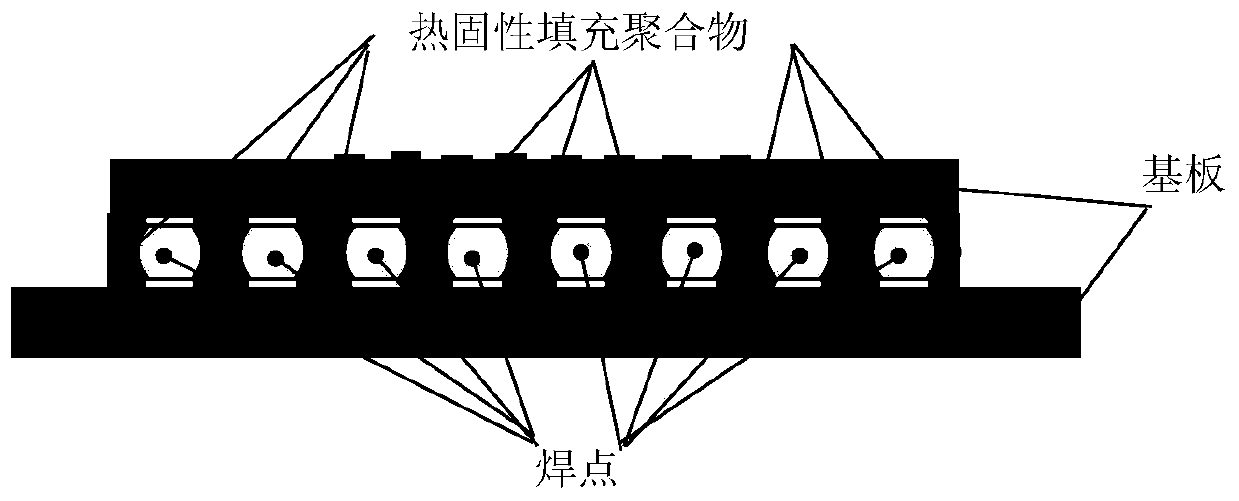
[0047] Such as figure 2 As shown, consider the electronic assembly as a three-layer assembly where the solder joints are sandwiched between substrates #1 and #2. The current practice is to fill the interlayer with solder joints of the same size and shape at equal axis distances. When the component experiences a temperature excursion ΔT, the distribution of the shear stress experienced by the solder joint is approximated by the formula where ε T is the differential thermal strain between the two substrates, l is the distance from the centerline to the edge of the electronic component, and x is the distance from the centerline; lambda x and κ s are the planar tensile compliance and shear compliance of the component, respectively, the formula The accuracy has been verified by finite element analysis method. An electronic component is a two-dimensional structure, although What is described is only the distribution of shear stress in the x direction, but the distributio...
Embodiment 2
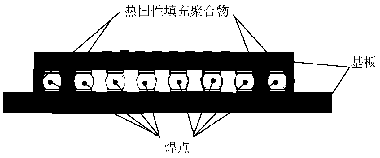
[0057] In this embodiment, based on optimizing the shear flexibility of the solder joints, the technical idea of making the solder joints from the center line to the edge of the electronic component have a more even distribution of shear force and moment. In this embodiment, the equivalent shear area of the solder joints is designed to be non-uniformly distributed from the center line to the edge of the electronic component - from large to small (such as Figure 7 shown). Equivalent shear area A of solder joint 3s , and the distribution in the x direction is: Among them, A 3o is the representative shear area at x=l.
[0058] At this point the shear compliance of the solder joint will be where κ o = h 3 p x p y / (G 3 A 3o ),G 3 is the shear modulus of the solder joint. At the same time, it is necessary to maintain the nodal area p x p y does not vary with x, so the shear force on the solder joint will be and the end moment will be M joint ≈F joint h 3 / ...
Embodiment 3
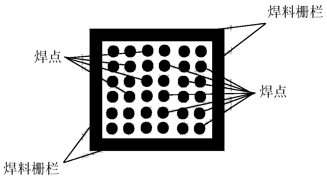
[0062] In this embodiment, based on optimizing the shear flexibility of the solder joints, the technical idea is to make the solder joints of the electronic component have a more even shear force and moment distribution from the center line to the edge. This embodiment designs the wheelbase area (being p x p y ) from the center line to the edge of the electronic component for non-uniform distribution – from dense to sparse (such as Figure 8 shown). Its distribution in the x direction is: where A po is the wheelbase area at x=l. At the same time, it is necessary to maintain the representative shear area of the solder joint (A 3s ) does not vary with x. Thus, the shear force on the solder joint will be and the end moment will be M joint ≈F joint h 3 / 2. Both do not vary with the x direction, such as Figure 8 shown.
[0063] The foregoing embodiments describe the mathematically optimal distribution of the axle-base area of solder joints along the x-direction ...
PUM
 Abstract
Description
Claims
Application Information