

A kind of resistive memory and preparation method thereof
A resistive memory and resistive layer technology, applied in electrical components and other directions, can solve the problems of small memory storage window and inability to meet forming-free characteristics, and achieve the effects of reducing manufacturing cost, saving time, and simplifying process flow
- Summary
- Abstract
- Description
- Claims
- Application Information
AI Technical Summary
Problems solved by technology
Method used
Image

Examples
Embodiment 1
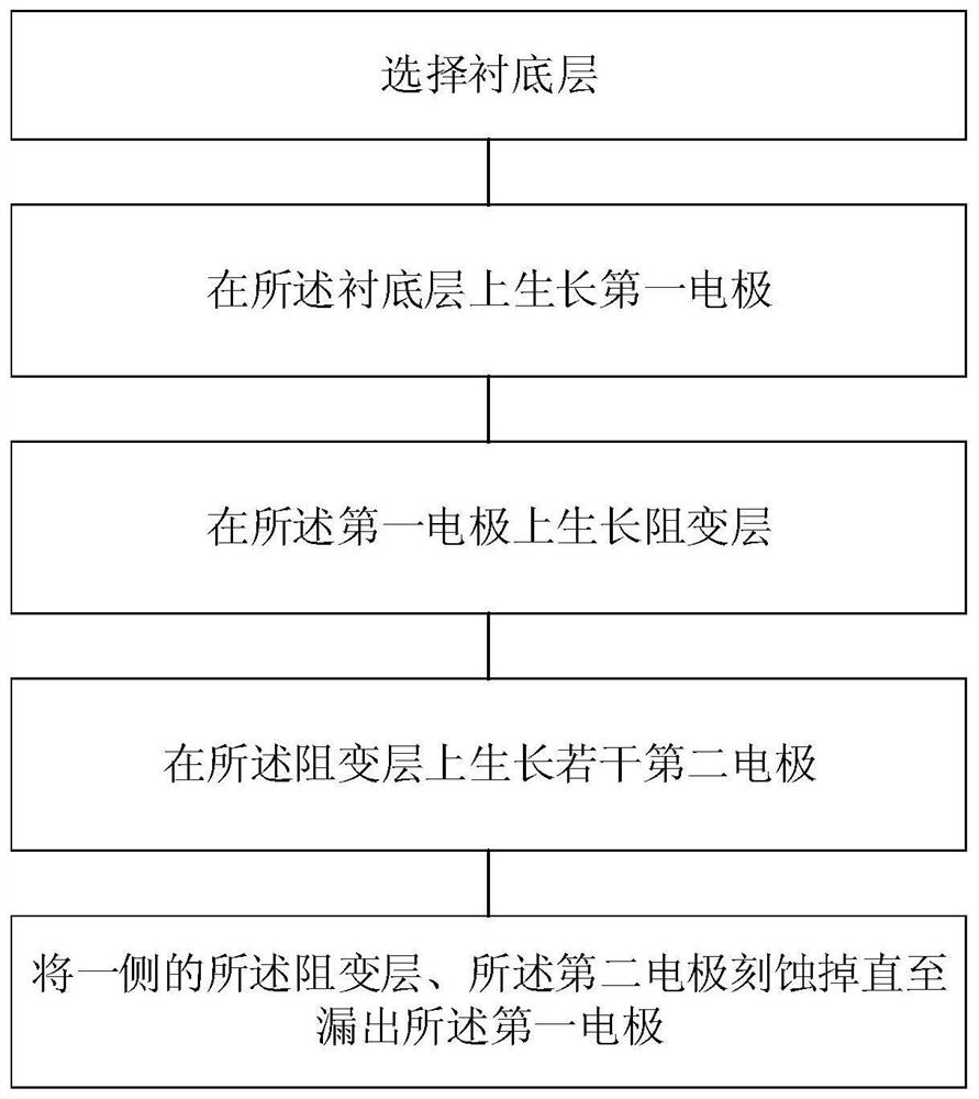
[0037] At present, the methods for optimizing device performance of resistive memory devices mainly include: designing multi-layer structures, changing material components by using different fabrication processes, and the like. Among them, in the multi-layer structure design, the overall current is usually reduced by adding a barrier layer, and the storage window of the resistive memory does not change significantly, and the operating voltage (including Set voltage and Reset voltage), forming voltage (resistive variable The voltage required for the initial opening of the memory, which is a large voltage) increases; in the use of different manufacturing methods to change the material composition, although the operating voltage and the storage window of the resistive memory do not increase significantly, it still needs to be formed. , and the process is more complicated.
[0038] Based on the existing questions above, see figure 1 , figure 1 This is a schematic flowchart of a ...
Embodiment 2
[0060] On the basis of the above Embodiment 1, please refer to Figures 2a to 2i , Figures 2a to 2i It is a schematic diagram of a manufacturing process flow of a resistive memory memory provided by an embodiment of the present invention. In this embodiment, a resistive memory in which the first electrode 3 is Pt, the second electrode 7 is Ta, and the dopant of the second resistive layer 5 is Ta is fabricated on the substrate layer 1. The specific preparation process of the resistive memory includes:
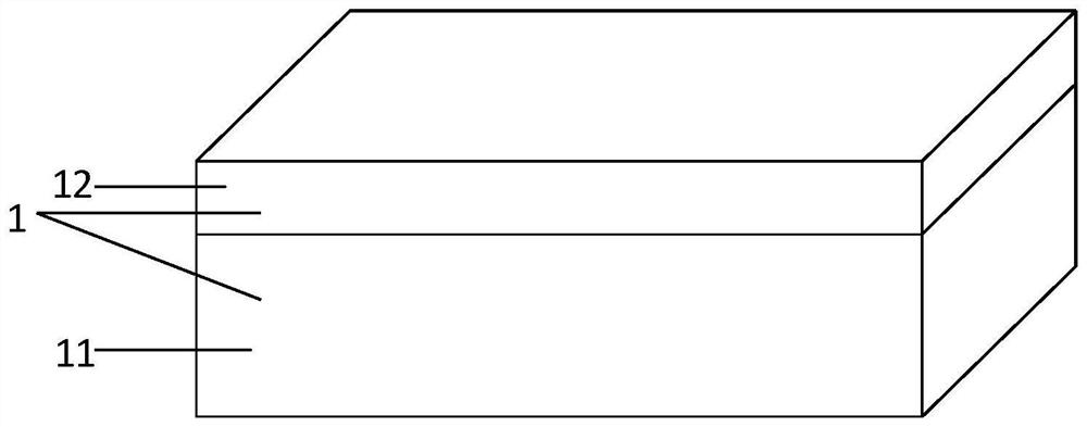
[0061] Step 1. Select the substrate layer 1.
[0062] see again Figure 2a , the substrate layer 1 selected in this embodiment is a composite substrate, and the selected substrate layer 1 is cleaned using the RCA standard cleaning process. The composite substrate includes a Si substrate layer 11 and SiO grown on the Si substrate layer 11 2 layer 12, the composite substrate may be a Si substrate layer 11 on which SiO has been grown 2 The existing composite substrate of laye...
Embodiment 3
[0085] On the basis of the second embodiment above, please refer to image 3 , image 3 It is a schematic structural diagram of a resistive memory provided by an embodiment of the present invention. This embodiment provides a resistive memory, the structure of the resistive memory includes from bottom to top: a substrate layer 1, an adhesive layer 2, a first electrode 3, a resistive layer, a second electrode 7, and a resistive layer It includes a first resistive switching layer 4 , a second resistive switching layer 5 , and a third resistive switching layer 6 in order from bottom to top. The resistive switching memory is prepared and formed by using the preparation methods described in the first and second embodiments.
[0086] The resistive memory provided in this embodiment has the technical effects described in Embodiment 1 and Embodiment 2 above, which will not be repeated here.
PUM
| Property | Measurement | Unit |
|---|---|---|
| thickness | aaaaa | aaaaa |
| thickness | aaaaa | aaaaa |
| thickness | aaaaa | aaaaa |
Abstract
Description
Claims
Application Information