
Ferroelectric double-annealing process capable of enhancing storage window

An annealing process, ferroelectric technology, applied in circuits, electrical components, electric solid-state devices, etc., can solve the problem of slow cell size scaling, and achieve the effect of large storage window and large storage window value

Pending Publication Date: 2022-01-04
SHANDONG UNIV
View PDF0 Cites 0 Cited by
  • Summary
  • Abstract
  • Description
  • Claims
  • Application Information

AI Technical Summary

Problems solved by technology

Cell size scaling is getting slower and slower due to patterning, leakage current and sensing margin challenges

Method used


Image

  • Ferroelectric double-annealing process capable of enhancing storage window
  • Ferroelectric double-annealing process capable of enhancing storage window
  • Ferroelectric double-annealing process capable of enhancing storage window

Examples


Embodiment 1

[0035] In this example, taking the ferroelectric memory based on hafnium oxide as an example, a new double annealing step process step is briefly described. Under the conditions of the same read and write times and the same read and write voltage, it has a larger storage window. Compared with the mainstream land, the device has good retention characteristics and a small operating voltage. It is a non-volatile memory with excellent performance.

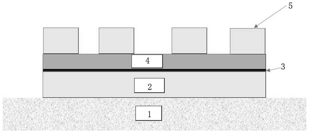
[0036] Figure 9 The flow chart of preparing the ferroelectric memory for this example includes 6 steps of preparing the lower motor, preparing the intercalation layer, pre-annealing the sample, preparing the functional layer, preparing the upper electrode and post-annealing the sample.

[0037] figure 1 The structure of the lower electrode 2 and the pre-annealing intercalation layer 3 is given. During the preparation process, the lower electrode 2 is first grown on a silicon-based or silicon dioxide substrate 1. This article uses m...

Embodiment 2

[0042] In this example, after the zirconia intercalation is prepared, the device is pre-annealed at a high temperature of 200 degrees Celsius. After the intercalation is prepared, the hafnium-zirconium-oxygen functional layer of 10 nanometers is grown in the atomic layer deposition (atomic layer deposition) instrument. In this step, 100 pulse cycles are grown (a single growth is larger than 0.1 nm), and the cycle method is superimposed growth of 5 hafnium oxide pulse cycles plus five zirconia pulse cycles, and then a triangle with a period of 1 millisecond is added to the upper and lower electrodes of the sample. Pulse, the pulse is first increased from 0V to 3V, then reduced from 3V to -3V, and then increased to 0V. Pulse waveform such as Figure 7 As shown, the period is 1 millisecond. The current is collected while the pulse is applied. After the current is collected, it is integrated, and the sum of the integrated current is divided by the area of ​​the electrode to conv...

Embodiment 3

[0044] In this embodiment, after the 2nm zirconia intercalation layer is grown, the sample is moved to a high-temperature rapid annealing furnace, and in a nitrogen atmosphere, the temperature is raised to 400 degrees Celsius at a rate of 20 degrees Celsius per second, and kept for one minute. Rapid anneal after one minute. When the temperature drops to 50 degrees Celsius, the sample is taken out, and then the functional layer is prepared. After the sample is taken out, the upper electrode is prepared, and finally annealed at the second high temperature. Move the sample into a high-temperature rapid annealing furnace, and raise the temperature to 500 degrees Celsius at a rate of 20 degrees Celsius per second in a nitrogen atmosphere, and keep it for one minute. Rapid anneal after one minute. When the temperature retreated to 50 degrees Celsius, the samples were taken out. Apply a triangular pulse with a period of 1 millisecond to the upper and lower electrodes of the sample....


PUM

PropertyMeasurementUnit
thicknessaaaaaaaaaa

Abstract

The invention discloses a ferroelectric double-annealing process capable of enhancing a storage window. According to the method, pre-annealing is carried out before a functional layer is grown on a ferroelectric memory, and post-annealing is carried out after an upper electrode is grown; the pre-annealing means that the memory on which the functional layer is to be grown is placed in an annealing furnace, the temperature is raised at the speed of V1 in the atmosphere of nitrogen, when the temperature reaches 200-500 DEG C, the temperature is kept for T1, after T1, rapid annealing is carried out, and when the temperature is reduced to 40-60 DEG C, the memory on which the functional layer is to be grown is taken out; and the post-annealing refers that the memory on which the upper electrode is grown is placed into an annealing furnace, the temperature is raised at a speed of V2 in a nitrogen atmosphere, the temperature for T2 is kept when the temperature reaches 400-700 DEG C, quick annealing is performed after T2, and the memory on which the upper electrode is grown is taken out when the temperature reaches 40-60 DEG C. Compared with a functional layer which is not pre-annealed, the semiconductor device has a larger storage window.

Description

technical field [0001] The invention relates to a pre-annealing process for one layer of a novel double-layer ferroelectric memory. Specifically, a new double-annealing process is designed to prepare a hafnium oxide-based novel ferroelectric memory. Background technique [0002] Major DRAM players such as Samsung, Micron, and SK hynix have produced DRAM cells down to the 15nm design rule (D / R). Now, they are developing n+1 and n+2 generations, the so-called 1a (or 1α) and 1b (or 1β), which means that the DRAM cell D / R with EUV may be able to shrink further below 12nm. Cell size scaling is getting slower and slower due to patterning, leakage current, and sensing margin challenges. Graphic DRAM and high-bandwidth memory (such as GDDR6(X) and HBM2(E)) use 20nm or 10nm-class DRAM technology nodes. By adding a low-power DRAM chip in the module, the camera module on the smartphone realizes the stacking of three chips. Some innovations can be seen in advanced DRAM products, such...

Claims


Application Information

Patent Timeline
Patent Type & Authority Applications(China)
IPC IPC(8): H01L21/324H01L27/11502H01L21/8239H10B53/00H10B99/00
CPCH01L21/324H10B53/00
Inventor 陈杰智台路魏巍
Owner SHANDONG UNIV
Learn More