A kind of three-dimensional structure nand ferroelectric storage unit and its preparation method
A technology of ferroelectric storage and three-dimensional structure, applied in the direction of electrical components, circuits, electric solid devices, etc., can solve problems such as interface layer degradation, improve fatigue resistance, improve storage performance and uniformity, and improve quality and uniformity Effect
- Summary
- Abstract
- Description
- Claims
- Application Information
AI Technical Summary
Problems solved by technology
Method used
Image
Examples
Embodiment 1
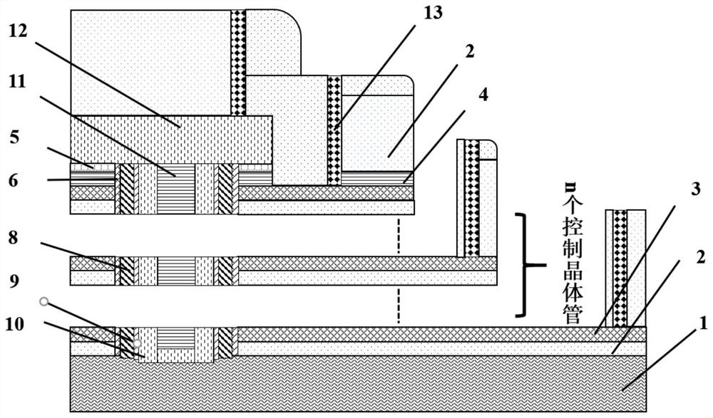
[0028] figure 1 It is a schematic cross-sectional structure diagram of a NAND ferroelectric memory cell with a three-dimensional structure provided in Embodiment 1 of the present invention.
[0029] Such as figure 1 As shown, the present embodiment provides a NAND ferroelectric memory cell, comprising: an oxide insulating layer, a channel layer, a channel buffer layer, a ferroelectric layer and a gate arranged in sequence from the inside to the outside; the channel A channel buffer layer is arranged between the ferroelectric layer and the ferroelectric layer; and / or, a gate buffer layer is arranged between the ferroelectric layer and the gate. Specifically, an oxide insulating layer, a channel layer, a channel buffer layer, a ferroelectric layer, and a gate buffer layer; or, an oxide insulating layer, a channel layer, a ferroelectric layer, and a gate buffer layer; or, an oxide insulating layer layer, channel layer, channel buffer layer and ferroelectric layer.
[0030] The...
Embodiment 2
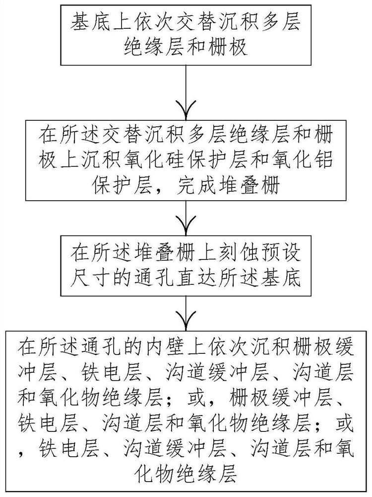
[0040] figure 2 is a flow chart of the manufacturing method of the three-dimensional structure NAND ferroelectric storage unit provided by the second embodiment of the invention.
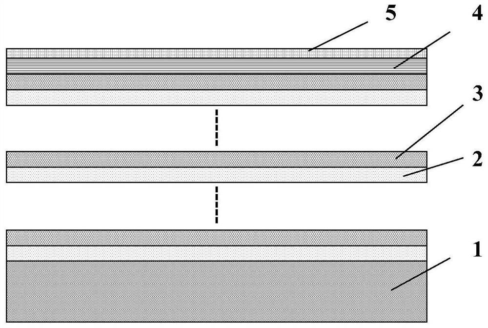
[0041] Such as figure 2 It is known that this embodiment provides a method for preparing a NAND ferroelectric memory unit, comprising: sequentially and alternately depositing multiple layers of insulating layers and gates on a substrate; depositing silicon oxide on the alternately deposited multiple layers of insulating layers and gates an insulating layer and an aluminum oxide insulating layer to complete the stacked gate; etching a via hole with a preset size on the stacked gate to reach the substrate; depositing a gate buffer layer, a ferroelectric layer, A channel buffer layer, a channel layer, and an oxide insulating layer; or, a gate buffer layer, a ferroelectric layer, a channel layer, and an oxide insulating layer; or, a ferroelectric layer, a channel buffer layer, a channel layer, and an...
PUM
| Property | Measurement | Unit |
|---|---|---|
| energy | aaaaa | aaaaa |
Abstract
Description
Claims
Application Information


