Method for preparing suede surface of single crystal silicon wafer

A monocrystalline silicon wafer and suede technology, applied in the field of solar cells, can solve problems such as unsuitable for industrial applications and unfavorable battery yields, and achieve the effect of simple and easy methods

Active Publication Date: 2019-10-29
TONGWEI SOLAR ENERGY CHENGDU CO LID
View PDF6 Cites 3 Cited by
  • Summary
  • Abstract
  • Description
  • Claims
  • Application Information

AI Technical Summary

Problems solved by technology

[0005] The purpose of the present invention is to solve the problem that when preparing the inverted pyramid suede surface of a single crystal cell, the medicinal solution often contains heavy metal ions that have a greater impact on the environment, and it is prepared by mechanical means, which has a great disadvantage to the battery yield. And it is not suitable for industrial application. Provide a method for preparing the textured surface of monocrystalline silicon wafers. The entire preparation process does not involve the existence of heavy metal ions, and will not cause additional pressure on waste liquid treatment; it does not need texture additives to assist texture production; The method is simple and easy, and the existing production line equipment can be directly used

Method used


Image

  • Method for preparing suede surface of single crystal silicon wafer

Examples


Embodiment 1

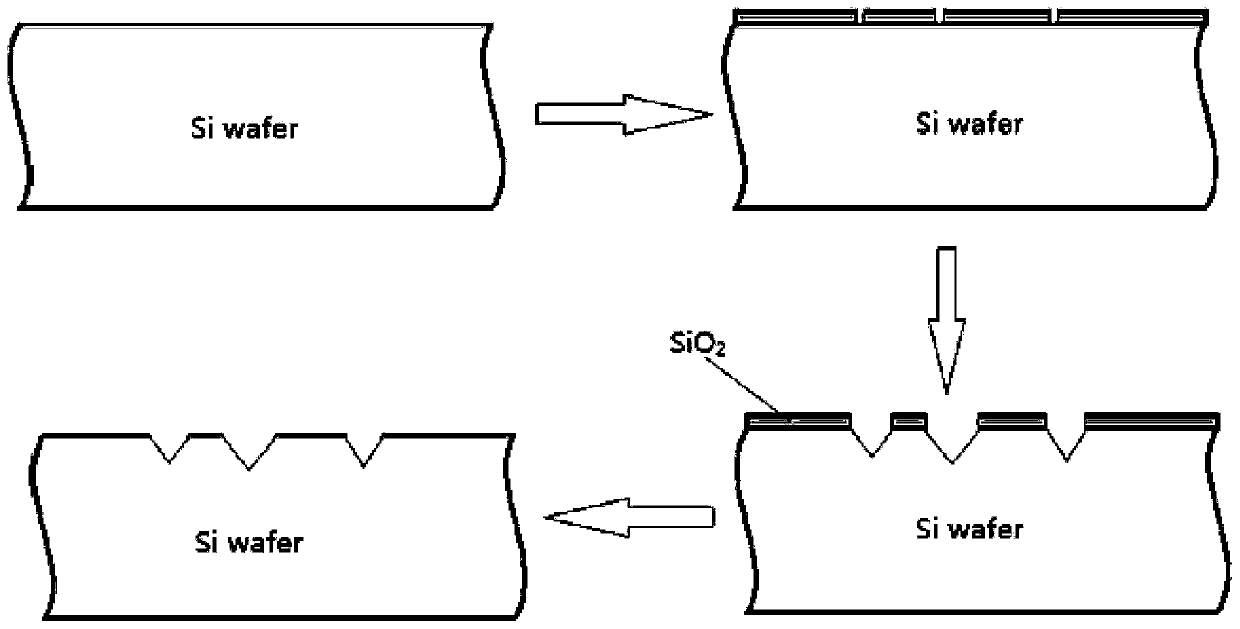
[0037] As shown in the figure, a method for preparing a textured surface of a single crystal silicon wafer includes the following steps:

[0038] (1) After pre-cleaning the monocrystalline silicon wafer with a cleaning solution to remove organic dirt on the surface, dry it;

[0039] (2) Carry out surface oxidation to the monocrystalline silicon slice obtained in step (1), produce oxide layer;

[0040] (3) performing high-temperature annealing on the monocrystalline silicon wafer obtained in step (2); the silicon oxide mask produces high-density pinholes after annealing, forming a channel for the direct contact reaction between the alkali solution and the silicon wafer;

[0041] (4) the monocrystalline silicon chip obtained in the step (3) is subjected to texturing; finally an inverted pyramid structure is formed at the pinhole position of the silicon oxide mask;

[0042] (5) removing the silicon oxide mask layer from the monocrystalline silicon wafer obtained in step (4), to ...


PUM

PropertyMeasurementUnit
thicknessaaaaaaaaaa
thicknessaaaaaaaaaa
sizeaaaaaaaaaa

Abstract

The invention discloses a method for preparing the suede surface of a single crystal silicon wafer. A novel method for preparing an inverted pyramidal suede structure by using a SiO2 mask is provided.According to the technical scheme, (1) organic smudge on the surface of the single crystal silicon wafer is removed; (2) surface oxidation is carried out on the single crystal silicon wafer acquiredin the step (1) to produce an oxide layer; (3) high temperature annealing is carried out on the single crystal silicon wafer acquired in the step (2); the silicon oxide mask generates a high-density pinhole after annealing, forming a channel in which an alkali solution directly contacts the silicon wafer; (4) the single crystal silicon wafer acquired in the step (3) is subjected to texturing, andfinally the inverted pyramidal structure is formed in the pinhole of the silicon oxide mask; and (5) the silicon oxide mask layer is removed from the single crystal silicon wafer acquired in the step(4) to acquire the desired inverted pyramidal suede. According to the invention, the inverted pyramidal suede is simply prepared based on the existing industrial manufacturing equipment without addingadditional consumption and introducing additional contaminating products.

Description

technical field [0001] The invention relates to the technical field of solar cells, in particular to a method for preparing a suede surface of a single crystal silicon wafer. Background technique [0002] In the current solar cell manufacturing process, the texturing of silicon wafers is an essential first step. A good textured structure can greatly improve the absorption of sunlight by the cell and increase the power generation capacity. In the current industrial process, lye and auxiliary additives are usually used to anisotropically etch the surface of the silicon wafer to form a dense pyramid-shaped suede structure, which can greatly reduce the surface reflection of the silicon wafer. Rate. However, the pyramid-shaped suede structure still has limitations: when the light is not direct and the ambient light is mostly scattered light, the light absorption rate is not good, and the protruding suede is more likely to be damaged by scratches in the subsequent process, result...

Claims


Application Information

Patent Timeline
Patent Type & Authority Applications(China)
IPC IPC(8): H01L31/18H01L21/308H01L21/306H01L21/67H01L31/0236
CPCH01L21/30604H01L21/3081H01L21/3086H01L21/67253H01L31/02363H01L31/1804Y02P70/50
Inventor 王涛张鹏杨蕾余波
Owner TONGWEI SOLAR ENERGY CHENGDU CO LID
Why Eureka
Try Eureka