A structure producing multiple surface lattice resonances and its application

A lattice and multiple technology, applied in the field of micro-nano photonic devices, can solve the problem of not being able to suppress the radiation loss of the system at the same time in multiple bands, and achieve the effect of suppressing the radiation loss of the system

Active Publication Date: 2021-10-19
TAIYUAN UNIV OF TECH
View PDF2 Cites 0 Cited by
  • Summary
  • Abstract
  • Description
  • Claims
  • Application Information

AI Technical Summary

Problems solved by technology

However, at present, a single surface lattice resonance can only regulate the spectrum in a single band, and cannot simultaneously suppress the radiation loss of the system in multiple bands, so that simultaneous modulation of multiple bands cannot be achieved.

Method used


Image

  • A structure producing multiple surface lattice resonances and its application
  • A structure producing multiple surface lattice resonances and its application
  • A structure producing multiple surface lattice resonances and its application

Examples


Embodiment 1

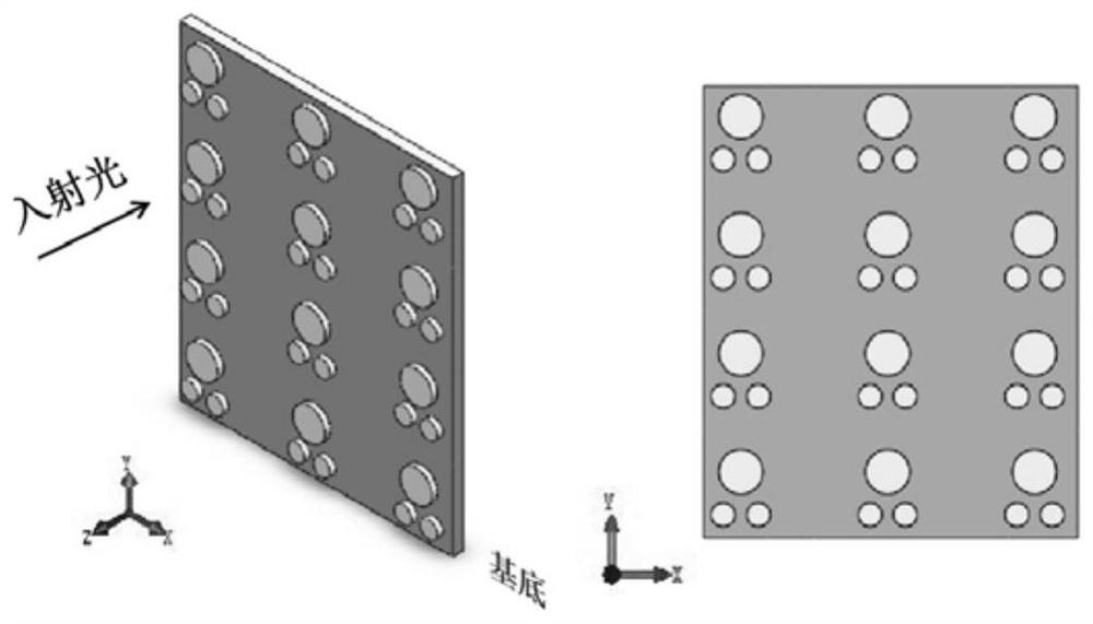
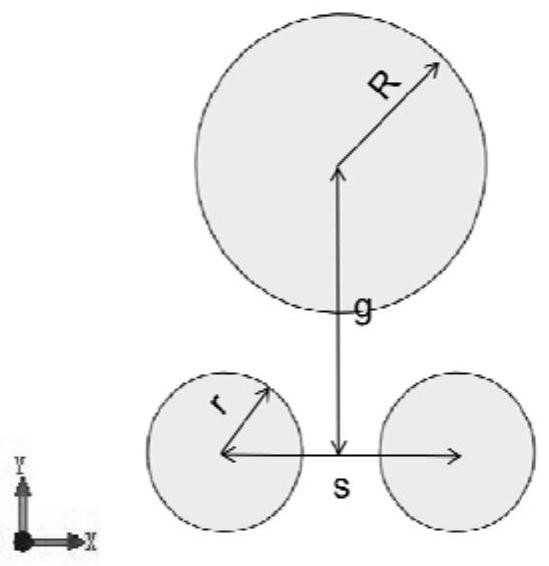
[0025] A structure generating multiple surface lattice resonances from a gold nanodisk trimer C 2V Molecules are arranged in an orderly array structure, such as figure 2 As shown, gold nanodisk trimer C 2V The molecule is composed of three gold nanodisks with the same thickness and different diameters. Among them, the diameters of the two small gold nanodisks are equal, the radius of the small gold nanodisk is r=80nm, the radius of the large gold nanodisk is R=150nm, s=240nm, g= 290nm, the thickness of both large and small gold nanodisks is h=50nm; figure 1 As shown, the above-mentioned array structure is etched on a quartz-PMMA (polymethyl methacrylate) substrate by ion / electron etching method, and a multi-mode surface plasmon laser chip is produced.

[0026] In order to test the performance of the above-mentioned plasmonic laser chip, through the electron beam etching experiment, the prepared sample was immersed in the oil matching the set refractive index for measurement...

Embodiment 2

[0028] A structure generating multiple surface lattice resonances from gold nanodisk tetramer C 2V Molecules are arranged in an orderly array structure, such as Figure 5 As shown, gold nanodisk tetramer C 2V The molecule is composed of four gold nanodisks, in which two small gold nanodisks have a radius of r=70nm, and two large gold nanodisks have a radius of R=90nm, s 1 =170nm,s 2 =240nm,s 3 =240nm, the thickness of the large and small gold nanodisks is h=50nm; if Figure 4 As shown, the above array structure is etched on the quartz-PMMA substrate by ion / electron etching method to make a multi-mode surface plasmon laser chip;

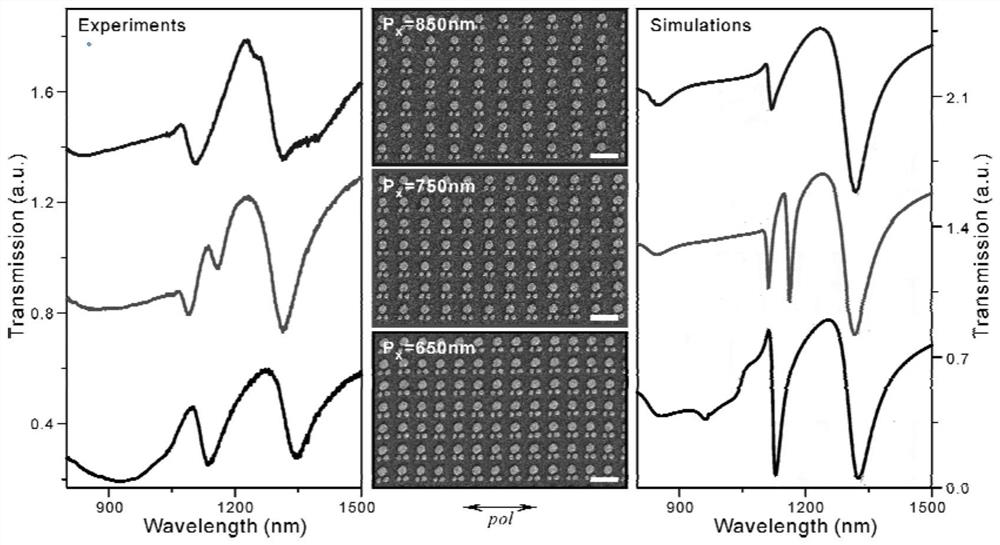
[0029] like Figure 6 As shown, electron beam etching experiments show that when the polarization direction of the incident field is in the x direction, the period P in the direction perpendicular to the polarization direction of the incident field is maintained y is 750nm, changing the period P in the polarization direction parallel to the inc...

Embodiment 3

[0031] A structure generating multiple surface lattice resonances from a gold nanodisk trimer D 3h Molecules are arranged in an orderly array structure, trimer D 3h The molecular point group is composed of three gold nanodisks of the same size. The radius of the gold nanodisk is set to r=80nm, the distance between the center of the gold nanodisk is s=175nm, and the thickness of the gold nanodisk is h=50nm. The above array structure is etched by ion / electron method etched on a quartz-PMMA substrate, such as Figure 7 As shown, the multi-mode surface plasmon laser chip is manufactured, the effect is the same as that of embodiment 1, and multiple surface lattice resonance can also be realized.


PUM

PropertyMeasurementUnit
radiusaaaaaaaaaa
thicknessaaaaaaaaaa
radiusaaaaaaaaaa

Abstract

The invention discloses a structure for generating multiple surface lattice resonance and its application, which belongs to the technical field of micro-nano photonic devices, and includes a substrate on which plasmonic molecules are arranged, and the plasmonic molecules have Arranged in an array structure, the plasmonic molecules are polymers composed of nano-gold or nano-silver unit structures; the plasmonic molecular array structure provided by the present invention can generate multiple surface lattice resonances, and the structure is used to make The formed surface plasmon laser chip can well excite multiple surface lattice resonances, and can suppress system radiation loss in multiple bands at the same time, modulate multiple bands, and emit nano-lasers in multiple bands. The development of information integration is of great significance.

Description

technical field [0001] The invention belongs to the technical field of micro-nano photonic devices, and in particular relates to a structure for generating multiple surface lattice resonances and an application thereof. Background technique [0002] Nano-laser is the frontier field developed by the combination of traditional semiconductor laser and micro-nano photonics, which is of great significance to the design of micro-nano photonic devices. At the same time, limited by the "three-dimensional optical diffraction limit", the development of integration and miniaturization of nano-lasers has been greatly challenged, but surface plasmon lasers can overcome the diffraction limit and limit light to sub-wavelength regions. At present, the surface plasmon laser system has a large radiation loss, which leads to a decrease in the quality factor and a weakening of the local field strength. [0003] Surface lattice resonance is a resonance mode excited by the coupling excitation of...

Claims


Application Information

Patent Timeline
Patent Type & Authority Patents(China)
IPC IPC(8): G02B5/00H01S5/30
CPCG02B5/008H01S5/30
Inventor 刘绍鼎刘杰岳鹏董红霞胡红刚耿伟贾卓楠刘钧妍栗正华
Owner TAIYUAN UNIV OF TECH
Why Eureka
Try Eureka