Perovskite oxide thin-film device, preparation method thereof and application thereof

A perovskite oxide and thin-film device technology, applied in the direction of electrical components, can solve problems such as the contradiction between erasing and writing speed and reliability, gate dielectric leakage, and limit the development of Flash memory, and achieve uniform surface microstructure, fewer holes, Ease of mass production

Pending Publication Date: 2019-11-05
GUANGDONG UNIV OF TECH
View PDF4 Cites 2 Cited by
  • Summary
  • Abstract
  • Description
  • Claims
  • Application Information

AI Technical Summary

Problems solved by technology

[0002] With the rapid development of electronic technology, the demand for non-volatile memory in the information field is also increasing. At present, Flash memory is the mainstream in the market. Howe

Method used


Image

  • Perovskite oxide thin-film device, preparation method thereof and application thereof
  • Perovskite oxide thin-film device, preparation method thereof and application thereof
  • Perovskite oxide thin-film device, preparation method thereof and application thereof

Examples


preparation example Construction

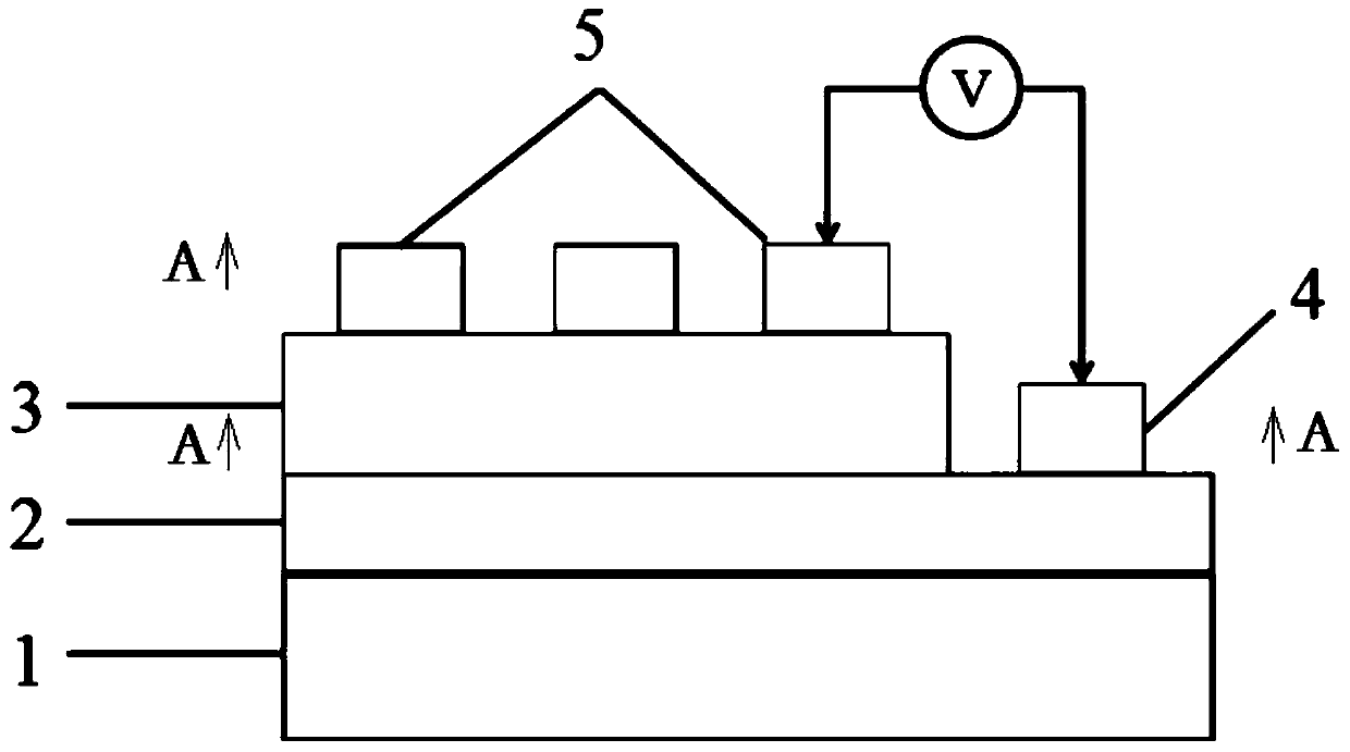
[0059] Specifically, the embodiment of the present application provides a method for preparing a perovskite oxide thin film device, including the following steps:

[0060] Step 1. According to the sol-gel method, the magnetron sputtering method, and the pulsed laser deposition method, the material of the bottom electrode layer is arranged on the surface of the base layer;

[0061] Step 2, according to sol-gel method, magnetron sputtering method, pulsed laser deposition method, PbZrO 3 layer is disposed on the surface of the bottom electrode on the side away from the base layer;

[0062] Step 3. Set the first top electrode on PbZrO 3 layer facing away from the surface of the side of the bottom electrode layer;

[0063] Step 4, disposing the second top electrode on the surface of the bottom electrode layer facing away from the base layer.

[0064] Among them, the sol-gel method, magnetron sputtering method or pulsed laser deposition method are all existing conventional method...

Embodiment 1

[0067] The embodiment of the present application adopts the sol-gel method to prepare perovskite oxide thin film devices, and the specific preparation process includes:

[0068] 1. Preparation of LaNiO 3 precursor solution and PbZrO 3 The precursor solution:

[0069] NeO 3 Precursor solution: the precursor solution is prepared with lanthanum nitrate hexahydrate La(NO 3 )36H 2 O, nickel acetate Ni(CH 3 COO) 24 h 2 O as a raw material was dissolved in ethylene glycol methyl ether and glacial acetic acid, respectively, and kept stirring at 50 °C until completely dissolved. When the temperature of the two bottles of solution drops to room temperature and there is no precipitation, mix the two solutions again, add acetylacetone dropwise as a stabilizer, and continue stirring at 50°C for 1 hour. After a completely clear and transparent solution is formed, use Ethylene glycol methyl ether and acetylacetone set the concentration of the solution to 0.25mol / L, and it can be used...


PUM

PropertyMeasurementUnit
Thicknessaaaaaaaaaa

Abstract

The invention relates to the technical field of electronic equipment and particularly relates to a perovskite oxide thin-film device, a preparation method thereof and application thereof. The perovskite oxide thin film device comprises a base layer, a bottom electrode layer, a PbZrO3 layer, a first top electrode and a second top electrode. The bottom electrode layer is disposed on a surface of thebase layer. The PbZrO3 layer is disposed on a surface of a side of the bottom electrode layer facing away from the base layer. The first top electrode is disposed on a surface of a side of the PbZrO3layer facing away from the bottom electrode layer. The second top electrode is disposed on a surface of a side of the bottom electrode layer facing away from the base layer. The purpose of the invention is to provide the perovskite oxide thin-film device with a high resistance switching ratio to improve the application range thereof.

Description

technical field [0001] The present application relates to the technical field of electronic equipment, in particular to a perovskite oxide thin film device and its preparation method and application. Background technique [0002] With the rapid development of electronic technology, the demand for non-volatile memory in the information field is also increasing. At present, the mainstream of the market is Flash memory, but due to the contradiction between the erasing speed and reliability of traditional Flash memory and the gate medium Problems such as electric leakage limit the development of Flash memory to a large extent. Therefore, the research and development of a new information storage technology has aroused extensive interest of researchers. Therefore, based on different material mechanisms, some new non-volatile memories have been developed, such as ferroelectric memory (FeRAM), magnetic memory (MRAM), phase change memory (PRAM) and resistive change memory (RRAM). R...

Claims


Application Information

Patent Timeline
IPC IPC(8): H01L45/00
CPCH10N70/8836H10N70/021H10N70/011
Inventor 王伦权李文华唐新桂
Owner GUANGDONG UNIV OF TECH
Why Eureka
Try Eureka