

Electronic packaging device and underfilling method
A technology for electronic packaging and devices, which is applied in the field of electronic packaging devices and their underfills. It can solve problems such as the difficulty of filling small gaps and the difficulty of filling materials with underfills, so as to reduce the risk of short circuits between pins and reduce thermal expansion. Coefficient difference, effect of reducing stress shock
- Summary
- Abstract
- Description
- Claims
- Application Information
AI Technical Summary
Problems solved by technology
Method used
Image

Examples
Embodiment 1
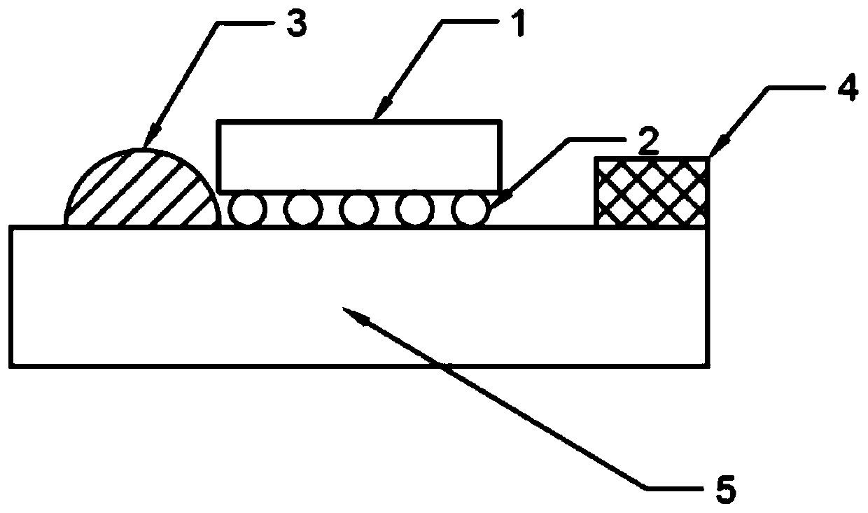
[0044] This embodiment provides an electronic packaging device, including an underfill glue 3, a substrate 5, a chip 1, and a solder ball 2; wherein, the underfill glue 3 includes bisphenol A type epoxy resin and a magnetic material Fe 2 o 3 , Fe 2 o 3 The particle size is 50μm, bisphenol A epoxy resin and Fe 2 o 3 The mass ratio of the substrate is 7:3; the substrate and the chip are connected by solder balls;
[0045] The filling method of the above-mentioned electronic packaging device, comprising,
[0046] Place the underfill on one side of the chip, and place the magnet on the other side of the chip, such as figure 1 , and then preheat the device to 40°C, under the combined action of the magnetic force of the magnet and the capillary effect, the underfill glue flows to the other side of the chip to fill the gap between the substrate and the chip, such as figure 2 , and then heated at 120° C. for 10 minutes to obtain a bottom-filled electronic packaging device.
Embodiment 2
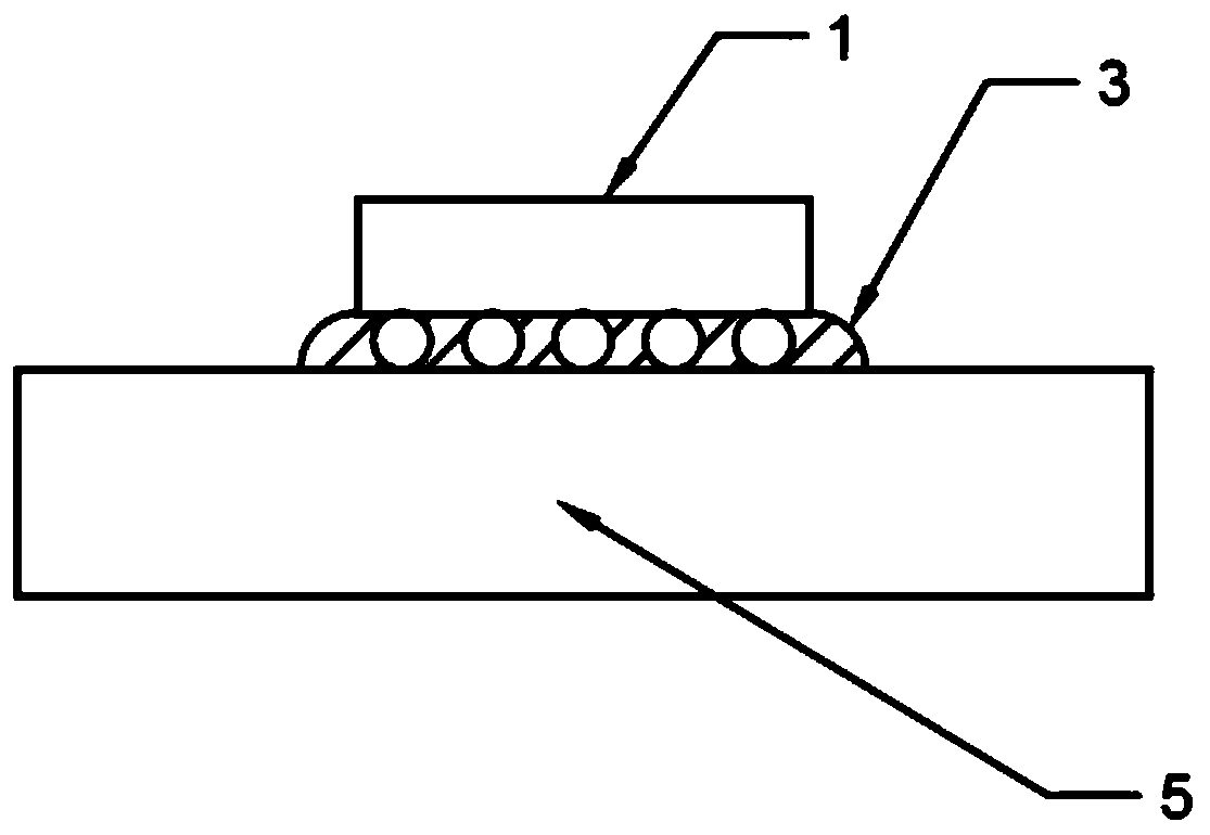
[0048] This embodiment provides an electronic packaging device, including an underfill glue 3, a substrate 5, a chip 1, and solder balls 2, wherein the underfill glue includes bisphenol A type epoxy resin and magnetic material CoFe 2 o 4 , bisphenol A epoxy resin and CoFe 2 o 4 The mass ratio is 1:1, CoFe 2 o 4 The particle size is 10nm, the CoFe in this embodiment 2 o 4 It uses atomic layer deposition technology to deposit a layer of SiO with a thickness of 1nm on its surface. 2 After modification, the substrate and the chip are connected by solder balls;
[0049] The filling method of the above-mentioned electronic packaging device, comprising,
[0050] Place the underfill on one side of the chip and the magnet on the bottom of the chip, see image 3 , and then preheat the device to 70°C, under the combined action of magnetic force and capillary effect, the underfill glue flows to the other side of the chip to fill the gap between the substrate and the chip, and then...
Embodiment 3
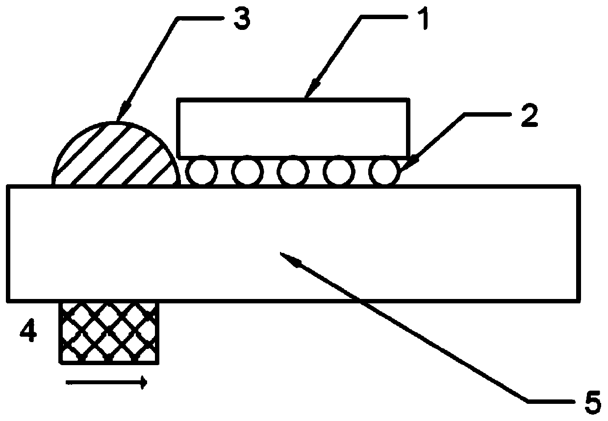
[0052] This embodiment provides an electronic packaging device, including an underfill glue 3, a substrate 5, a motherboard 6, and solder balls 2; wherein the underfill glue includes tetraphenol ethane tetraglycidyl ether epoxy resin, magnetic material nickel And silicon dioxide, the mass ratio of tetraphenol ethane tetraglycidyl ether epoxy resin, nickel and silicon dioxide is 8:1:1, and the nickel particle diameter is 500nm, and the nickel in the present embodiment adopts coupling agent γ-Aminopropyltriethoxysilane is used after surface treatment, and the substrate and the motherboard are connected by solder balls;
[0053] The filling method of the above-mentioned electronic packaging device, comprising,
[0054] Place the underfill on one side of the motherboard and the magnet on the other side of the motherboard, see Figure 4 , and then preheat the device to 60°C. Under the joint action of magnetic force and capillary effect, the underfill glue flows to the other side o...
PUM
 Abstract
Description
Claims
Application Information