Gate structure, manufacturing method of gate structure, and enhanced semiconductor device

A gate structure and gate electrode technology, applied in semiconductor devices, semiconductor/solid-state device manufacturing, electrical components, etc., can solve problems such as low turn-on voltage, insufficient hole concentration, uneven device turn-on voltage and on-resistance, etc. , to increase the turn-on voltage, improve uniformity and repeatability

Active Publication Date: 2019-11-08
GUANGDONG INST OF SEMICON IND TECH
View PDF4 Cites 6 Cited by
  • Summary
  • Abstract
  • Description
  • Claims
  • Application Information

AI Technical Summary

Problems solved by technology

The turn-on voltage of the device depends on the hole concentration in the p-type gate, and a higher turn-on voltage requires a higher hole concentration, but since p-GaN or p-AlGaN is usually doped with magnesium (Mg), and The doping concentration and activation rate of Mg are limited, resulting in insufficient hole concentration, which in turn leads to a low turn-on voltage of the device (less than 3V).
[0004] In device manufacturing, the patterning of the p-type gate is usually formed by ion etching. However, due to the lack of effective selective etching process between the p-GaN or p-AlGaN layer and the AlGaN layer under the gate, it is difficult to precisely control The thickness and uniformity of etching lead to non-uniform turn-on voltage and on-resistance of devices on the entire wafer, and the manufacturing process repeatability is also poor

Method used


Image

  • Gate structure, manufacturing method of gate structure, and enhanced semiconductor device
  • Gate structure, manufacturing method of gate structure, and enhanced semiconductor device
  • Gate structure, manufacturing method of gate structure, and enhanced semiconductor device

Examples


no. 1 example

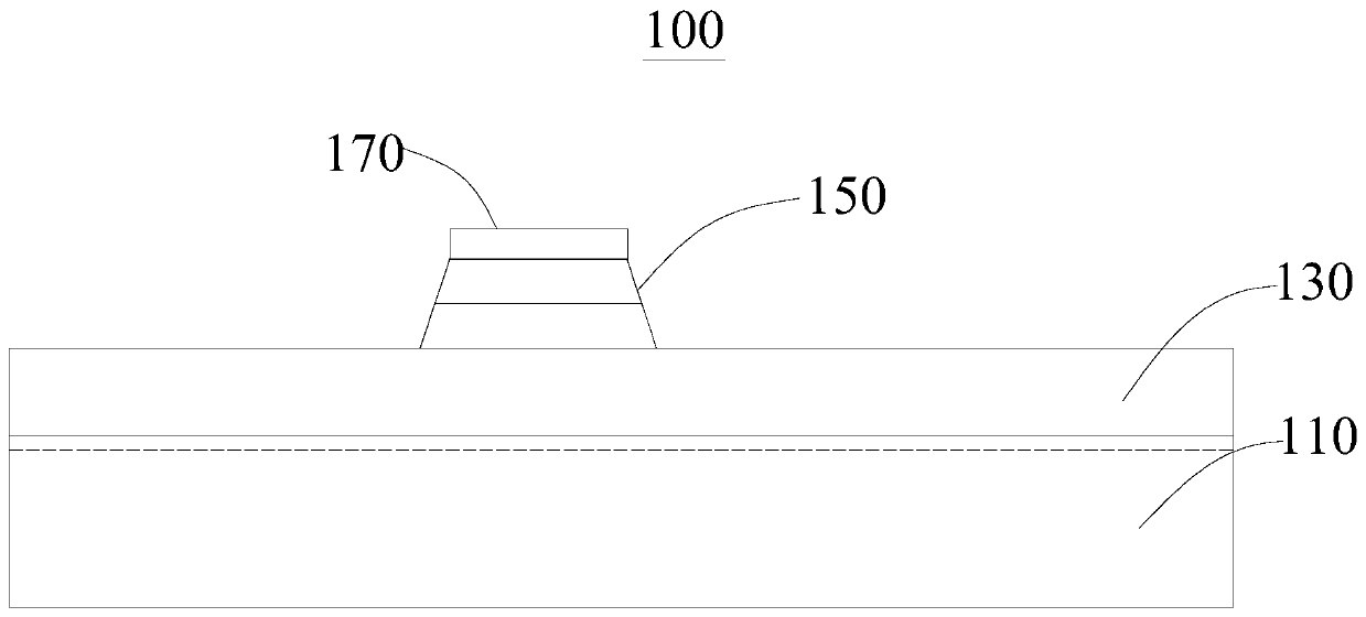
[0046] Please refer to figure 1 , this embodiment provides a gate structure 100 that can increase the turn-on voltage and improve the applicability of the overall device. The gate structure 100 is a part of the enhanced GaN HEMT device structure, and the enhanced GaN HEMT device also includes a support layer 200 , a source electrode and a drain electrode. For the specific structure of the enhanced GaN HEMT device, please refer to subsequent embodiments.

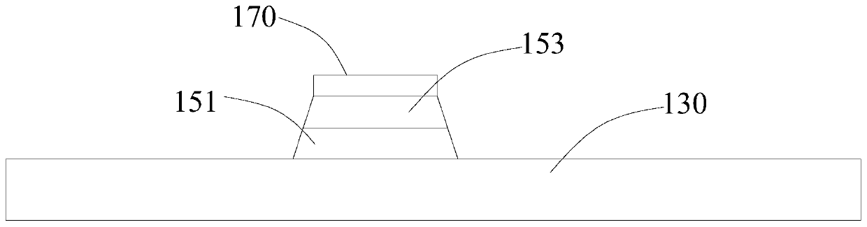
[0047] The gate structure 100 provided in this embodiment includes: a channel layer 110, a barrier layer 130 disposed on the channel layer 110, a cap layer 150 disposed on the barrier layer 130, and a gate electrode disposed on the cap layer 150 layer 170 , wherein the cap layer 150 has a crystal polarization orientation opposite to that of the barrier layer 130 . The channel layer 110 is used to be disposed on a substrate, and a passivation layer 500 is also disposed on the cap layer 150 and part of the barrier layer 130. F...

no. 2 example

[0070] see Figure 4 , this embodiment provides an enhanced semiconductor device 10, including a support layer 200, a gate structure 100, a source electrode layer 300, and a drain electrode layer 400, wherein the basic structure and principle of the gate structure 100 and the resulting technical effects and The first embodiment is the same, and for brief description, for parts not mentioned in this embodiment, reference may be made to the corresponding content in the first embodiment.

[0071] The gate structure 100 includes: a channel layer 110, a barrier layer 130 disposed on the channel layer 110, a cap layer 150 disposed on the barrier layer 130, and a gate electrode layer 170 disposed on the cap layer 150, wherein, The cap layer 150 has an opposite crystal polarization orientation to the barrier layer 130 . The channel layer 110 is disposed on the support layer 200 , and the source electrode layer 300 and the drain electrode layer 400 are both disposed on the barrier lay...


PUM


Abstract

A gate structure, a manufacturing method of the gate structure, and an enhanced semiconductor device relate to the semiconductor technology field. The gate structure includes a channel layer, a barrier layer arranged on the channel layer, a cap layer arranged on the barrier layer, and a gate electrode layer arranged on the cap layer. The cap layer has a crystal polarization orientation which is opposite to the barrier layer. A cap layer material with an opposite polarity orientation of the barrier layer is used so that an interface between the barrier layer and the cap layer has extremely strong negatively polarized charges and a conduction band energy level is bent upwardly. The conduction band energy level of the barrier layer and the channel layer is raised above a Fermi level, a two-dimensional electron gas/two-dimensional cavity gas at the interface between the barrier layer and the channel layer can be effectively exhausted so as to increase a turn-on voltage. Simultaneously, different chemical properties of different crystal polarization orientations are used to realize self-termination wet etching of a gate pattern so as to increase uniformity and repeatability of device manufacturing.

Description

technical field [0001] The present invention relates to the technical field of semiconductors, in particular to a gate structure, a manufacturing method of the gate structure and an enhanced semiconductor device. Background technique [0002] Due to the large band gap of gallium nitride (GaN) materials, power semiconductor devices based on GaN materials can have higher breakdown voltage and higher power density than traditional silicon (Si)-based power devices; Using the inherent polarization characteristics of GaN materials, a two-dimensional electron gas channel with high concentration and high electron mobility can be formed, so it can have a higher switching frequency than traditional silicon-based power devices. AlGaN / GaN high-mobility transistors (HEMTs) with a planar structure based on GaN's high withstand voltage and high-frequency characteristics have a wide range of application requirements in the high-voltage and high-frequency fields. [0003] In the prior art, ...

Claims


Application Information

Patent Timeline
Patent Type & Authority Applications(China)
IPC IPC(8): H01L29/43H01L21/28H01L29/778H01L21/335
CPCH01L29/432H01L21/28H01L29/7786H01L29/66462
Inventor 李成果任远
Owner GUANGDONG INST OF SEMICON IND TECH
Why Eureka
Try Eureka