High-precision ultrathin solder mask layer on surface of LTCC substrate and manufacturing process method thereof

A technology of substrate surface and manufacturing process, which is applied to the photoengraving process of pattern surface, the coating equipment of photoengraving process, the exposure device of photoengraving process, etc. problems, to achieve the effect of mature process technology and materials, firm adhesion and easy realization

Inactive Publication Date: 2019-11-29
SOUTHWEST CHINA RES INST OF ELECTRONICS EQUIP
View PDF10 Cites 0 Cited by
  • Summary
  • Abstract
  • Description
  • Claims
  • Application Information

AI Technical Summary

Problems solved by technology

[0005] It can be known from public reports that most of the current PCB solder mask layers are produced by screen printing and light curing. The thickness of the solder mask layer is generally above 20 μm, and it is difficult to control the uniform thickness, which is not conducive to chip precision. bump soldering
And the manufacture of high-precision micro-opening solder mask layers with openings below 0.1mm has not received special attention, and there is no public report on the matching application of such solder mask materials and LTCC substrates.

Method used


Image

  • High-precision ultrathin solder mask layer on surface of LTCC substrate and manufacturing process method thereof
  • High-precision ultrathin solder mask layer on surface of LTCC substrate and manufacturing process method thereof
  • High-precision ultrathin solder mask layer on surface of LTCC substrate and manufacturing process method thereof

Examples


Embodiment 1

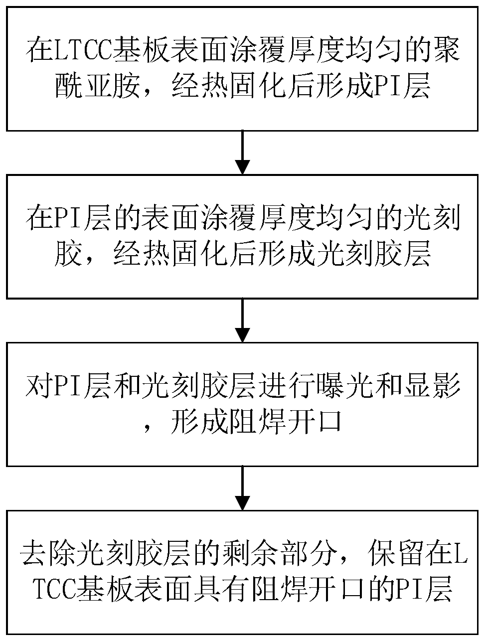
[0054] A method for manufacturing a high-precision ultra-thin solder mask layer on the surface of an LTCC substrate 1 provided in this embodiment includes the following steps:

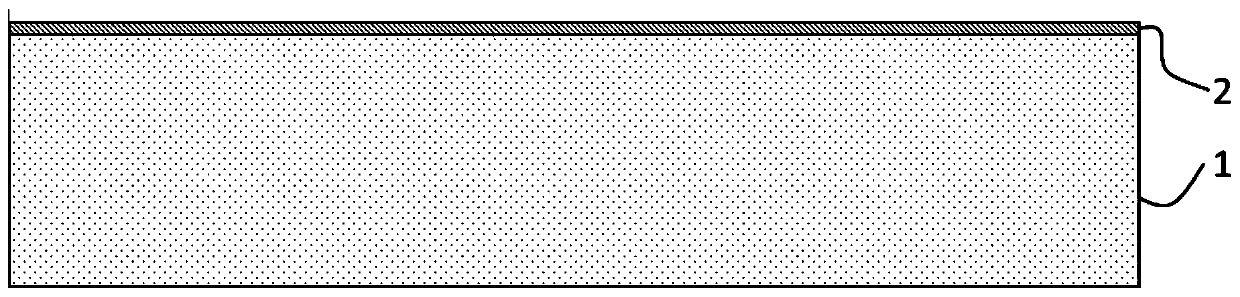
[0055] Step 1: Coating polyimide with a uniform thickness on the surface of the LTCC substrate 1, and forming a PI layer after thermal curing. 2: Using the spin coating method, set the spin coating speed to 3000 rpm, and spin coating for 20 seconds. The surface of the LTCC substrate 1 is coated with polyimide with a uniform thickness, and the coated polyimide is dried at 90°C for 20 minutes. After the coated polyimide is dried and cured, a thickness of PI layer 2 of 4 μm.

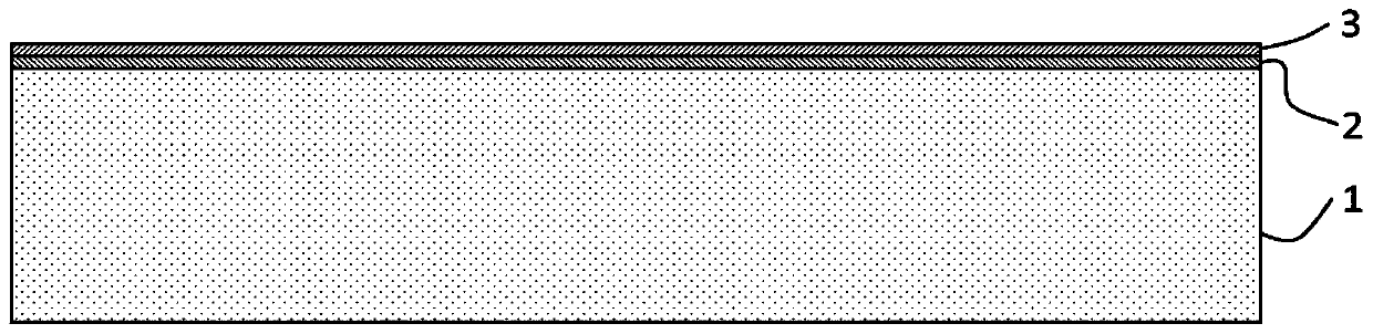
[0056] Step 2, coating photoresist with uniform thickness on the surface of PI layer 2, and forming photoresist layer 3 after thermal curing: adopt spin coating method, set spin coating speed to 1000 rpm, and spin coating for 30 seconds , coating a photoresist with a uniform thickness on the surface of the PI layer 2, drying the co...

Embodiment 2

[0063] A method for manufacturing a high-precision ultra-thin solder mask layer on the surface of an LTCC substrate 1 provided in this embodiment includes the following steps:

[0064] Step 1: Coating polyimide with a uniform thickness on the surface of the LTCC substrate 1, and forming a PI layer after thermal curing. 2: Using the spin coating method, set the spin coating speed to 2500 rpm, and spin coating for 15 seconds. The surface of the LTCC substrate 1 is coated with polyimide with a uniform thickness, and the coated polyimide is dried at 100°C for 15 minutes. After the coated polyimide is dried and cured, a thickness of PI layer 2 of 5 μm.

[0065] Step 2: Coating photoresist with uniform thickness on the surface of PI layer 2, forming photoresist layer 3 after thermal curing: using spin coating method, setting the spin coating speed to 2200 rpm, spin coating for 10 seconds , coating a photoresist with a uniform thickness on the surface of the PI layer 2, drying the c...

Embodiment 3

[0073] A method for manufacturing a high-precision ultra-thin solder mask layer on the surface of an LTCC substrate 1 provided in this embodiment includes the following steps:

[0074] Step 1: Coating polyimide with a uniform thickness on the surface of the LTCC substrate 1, and forming a PI layer after thermal curing. 2: Using the spin coating method, set the spin coating speed to 2000 rpm, and spin coating for 10 seconds. The surface of the LTCC substrate 1 is coated with polyimide with a uniform thickness, and the coated polyimide is dried at 120°C for 10 minutes, and the coated polyimide is dried and cured to form a thickness of PI layer 2 of 7 μm.

[0075] Step 2: Coating photoresist with uniform thickness on the surface of PI layer 2, forming photoresist layer 3 after thermal curing: using spin coating method, setting the spin coating speed to 2500 rpm, spin coating for 10 seconds , coating a photoresist with a uniform thickness on the surface of the PI layer 2, drying ...


PUM

PropertyMeasurementUnit
thicknessaaaaaaaaaa
thicknessaaaaaaaaaa
thicknessaaaaaaaaaa

Abstract

The invention discloses a high-precision ultrathin solder mask layer on the surface of an LTCC substrate and a manufacturing process method thereof. The manufacturing process method comprises the steps of: 1, coating polyimide with uniform thickness on the surface of an LTCC substrate, and forming a PI layer after thermocuring; 2, coating photoresist with uniform thickness on the surface of the PIlayer, and forming a photoresist layer after thermocuring; 3, exposing and developing the PI layer and the photoresist layer to form a solder mask opening; and 4, removing the remaining part of the photoresist layer, and reserving the PI layer with the solder mask opening on the surface of the LTCC substrate. According to the invention, a photoetching process technology is used on the surface ofthe LTCC substrate, polyimide serves as a medium to manufacture the high-precision ultrathin solder mask layer, the size of the solder mask opening can be as small as 50 [mu]m, the precision of the size and the position of the opening is superior to +/-5 [mu]m, the thickness of the solder mask layer is smaller than 10 [mu]m, the solder mask layer is firmly attached to the surface of the substrate,and back-off welding of the LTCC substrate and a high-density bare chip can be well supported.

Description

technical field [0001] The invention relates to the technical field of LTCC substrate manufacturing, in particular to a high-precision ultra-thin solder mask layer on the surface of an LTCC substrate and a manufacturing process thereof. Background technique [0002] LTCC technology can achieve excellent high-frequency performance, high integration density and high reliability, and has been widely used in electronic information equipment platforms such as airborne, missile-borne, and space-borne. With the further improvement of the miniaturization and lightweight requirements of the whole system, the RF functional units and high-density digital packaging units must achieve smaller volumes and more compact interconnection forms. Traditional chip packaging, gold wire / gold ribbon interconnection, The hybrid integration method composed of metal box hermetic packaging can no longer meet the product requirements well, and the SIP packaging form of high-density bare chip and substra...

Claims


Application Information

Patent Timeline
Patent Type & Authority Applications(China)
IPC IPC(8): H05K3/34G03F7/16G03F7/20G03F7/32G03F7/42G03F9/00
CPCG03F7/162G03F7/168G03F7/2004G03F7/322G03F7/422G03F9/00H05K3/3452
Inventor 岳帅旗王春富王娜王贵华伍泽亮
Owner SOUTHWEST CHINA RES INST OF ELECTRONICS EQUIP
Why Eureka
Try Eureka