A fabrication method of pixel-level on-chip spectroscopy chip based on metasurface structure

A metasurface, pixel-level technology, applied in the field of micro-nano photonics device preparation, can solve the problems of narrow working band range, complex preparation process, and the inability of image sensors to correspond one-to-one pixels. Information collection, flexible design effects

Active Publication Date: 2022-02-08
苏州施密科微电子设备有限公司 +1
View PDF3 Cites 0 Cited by
  • Summary
  • Abstract
  • Description
  • Claims
  • Application Information

AI Technical Summary

Problems solved by technology

Although through research in recent years, infrared detectors can basically correspond to pixels, image sensors at visible light wavelengths still cannot achieve one-to-one correspondence with pixels, and a single F-P cavity can only achieve monochromatic spectrum collection. The tunable F-P cavity is limited to the micro-electromechanical system to adjust the cavity length of the F-P to achieve light splitting during the image acquisition process. The working band range is relatively narrow and can only work in a specific wavelength range. Secondly, the F-P cavity filter is tuned by moving parts. It takes a long time to realize, and the overall device integration preparation process is complex

Method used


Image

  • A fabrication method of pixel-level on-chip spectroscopy chip based on metasurface structure
  • A fabrication method of pixel-level on-chip spectroscopy chip based on metasurface structure

Examples


Embodiment

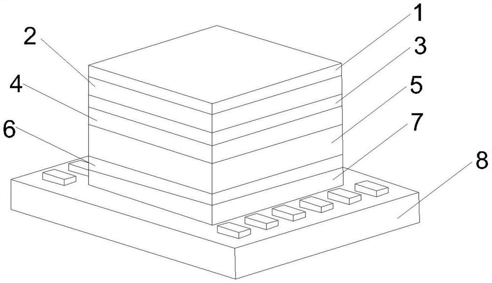
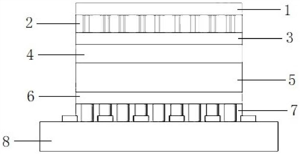
[0031] Such as Figure 1-2 As shown, a method for preparing a pixel-level on-chip spectrum chip process based on a metasurface structure is characterized in that it comprises the following steps:

[0032] S1: In the cap layer InP of the InP / InGaAs / InP material, Zn diffusion process, ultraviolet lithography process and electron beam evaporation process are used to prepare the pixel, P-type metal electrode and overlay mark of the detector;

[0033] S2: N-type metal electrodes are prepared in the cap layer InP of InP / InGaAs / InP material by wet etching process and electron beam evaporation process;

[0034] S3: Thinning and polishing process is carried out on the substrate InP of InP / InGaAs / InP material, and a dielectric layer is passivated by plasma chemically enhanced vapor deposition on the polished InP surface, and a dielectric layer is deposited on the surface of the dielectric layer by low-pressure chemical deposition growing monocrystalline silicon;

[0035] S4: Prepare a...


PUM


Abstract

The invention discloses a method for preparing a pixel-level on-chip spectral chip based on a metasurface structure, which uses processes such as ultraviolet lithography, diffusion, electron beam evaporation coating, and etching to prepare broadband InGaAs photosensitive chips on InP / InGaAs / InP materials. element, using nanoimprinting, reactive ion etching, low-pressure chemical deposition and other processes to integrate and prepare pixel-level micro-filter arrays. The micro-filter units correspond to photosensitive elements one by one. It is precisely connected with the broadband InGaAs photosensitive element integrated micro-filter array. Beneficial effects of the present invention: It is suitable for the miniaturization requirements of spectral imagers, realizes the collection of fine map information, designs and prepares multi-channel narrow-band filters according to the characteristic wavelengths of different observed objects, realizes spectral imaging of different measured targets, and is compatible with MEMS technology Secondly, the nanoimprinting process is used to make the batch preparation cost low, which is conducive to popularization and application.

Description

technical field [0001] The invention relates to technology belonging to the field of preparation of micro-nano photonics devices, in particular to an integrated preparation technology of an on-chip spectrum chip, specifically a pixel-level on-chip spectrum chip process preparation method based on a metasurface structure. Background technique [0002] Imaging spectrometers are the core of spectral imaging technology. Traditional spectrometers use dispersive elements such as prisms or gratings to separate spectral bands, and the spectra of different bands are imaged on different detectors. Due to the light dispersion ability of the spectroscopic element and the limitation of the pixel size of the detector, in a traditional spectrometer, the detector needs to be at a certain distance from the spectroscopic element to effectively distinguish and receive the spectrum, resulting in a relatively large overall size of the spectrometer . In addition, due to the discrete layout of th...

Claims


Application Information

Patent Timeline
Patent Type & Authority Patents(China)
IPC IPC(8): H01L27/146
CPCH01L27/14625H01L27/14621H01L27/14636H01L27/14685H01L27/14687
Inventor 仝晓刚
Owner 苏州施密科微电子设备有限公司
Why Eureka
Try Eureka