Method for epitaxial growth of gallium nitride (GaN) thin film on Si substrate

An epitaxial growth and substrate technology, applied in coating, gaseous chemical plating, metal material coating process, etc., can solve the problems of difficult realization and complex growth process, improve the quality of epitaxy, simplify the growth process, and be easy to realize Effect

Inactive Publication Date: 2019-12-06
WENZHOU UNIVERSITY +1
View PDF2 Cites 9 Cited by
  • Summary
  • Abstract
  • Description
  • Claims
  • Application Information

AI Technical Summary

Problems solved by technology

However, using the above methods to epitaxially grow GaN thin films, the growth process is relatively complicated, and it is relatively difficult to realize

Method used


Image

  • Method for epitaxial growth of gallium nitride (GaN) thin film on Si substrate
  • Method for epitaxial growth of gallium nitride (GaN) thin film on Si substrate
  • Method for epitaxial growth of gallium nitride (GaN) thin film on Si substrate

Examples


Embodiment Construction

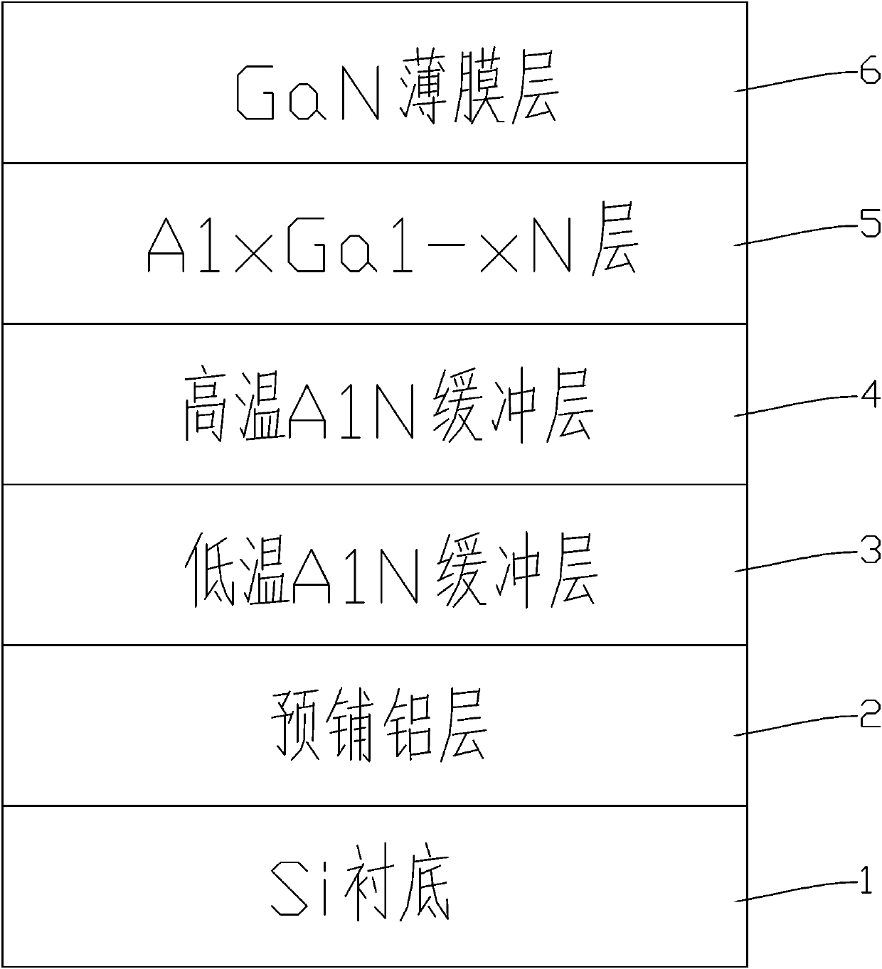
[0028] refer to Figure 1-4 As shown, the method for epitaxially growing a GaN thin film on a Si substrate of the present invention adopts an MOCVD system for epitaxial growth. Its epitaxial structure is Si substrate 1, pre-coated aluminum layer 2, low-temperature AlN buffer layer 3, high-temperature AlN buffer layer 4, Al x Ga 1-xN layer 5 and GaN thin film layer 6. Among them: the low-temperature AlN buffer layer 3 is a low-temperature AlN three-dimensional nucleation layer, the high-temperature AlN buffer layer 4 is a high-temperature AlN two-dimensional nucleation layer, the AlxGa1-xN layer 5 is an AlxGa1-xN stress release layer, and the GaN film layer 6 is the final growth layer . As mentioned above, AlN is aluminum nitride, AlxGa1-xN is aluminum gallium nitride, and GaN is gallium nitride. During the growth process, TMGa (trimethylgallium) and TMAl (trimethylaluminum) are used as Ga sources respectively (Ga (gallium) atoms cleaved from trimethylgallium at high temper...


PUM

PropertyMeasurementUnit
thicknessaaaaaaaaaa

Abstract

The invention relates to a method for epitaxial growth of a gallium nitride (GaN) thin film on a Si substrate, the crack growth of GaN epitaxial thin films is limited, the surface topography is uniform, the process is relatively easy, and the method is easy to realize. According to the technical scheme, the method includes the steps that a metal-organic chemical vapor deposition (MOCVD) system isadopted for epitaxial growth and the epitaxial growth of the GaN thin film is conducted on the Si substrate. The method is characterized in that the epitaxial structure of the GaN thin film sequentially comprises the Si substrate, a pre-buried aluminum layer, a low temperature aluminum nitride (AlN) buffer layer, a high temperature aluminum nitride (AlN) buffer layer, a gallium nitride aluminum (AlxGal-xN) layer and the GaN thin film layer, wherein the low temperature AlN buffer layer is a low temperature AlN three-dimensional nucleating layer, the high temperature AlN buffer layer is a high temperature AlN three-dimensional nucleating layer, the AlxGal-xN layer is an AlxGal-xN stress relief layer, and the GaN thin film layer is a final growth layer.

Description

technical field [0001] The invention belongs to the technical field of semiconductor thin film materials, in particular to a method for epitaxially growing gallium nitride (GaN) thin films on silicon (Si) substrates. Background technique [0002] The third-generation wide-bandgap direct-gap semiconductor material represented by GaN is a new type of semiconductor material that has attracted international attention in recent years. It has excellent physical and chemical stability, high saturation electron drift velocity, high breakdown field strength and Superior properties such as high thermal conductivity make it the most preferred material for short-wavelength semiconductor optoelectronic devices and high-frequency, high-voltage, high-temperature microelectronic devices. [0003] Traditionally, the substrates for growing GaN thin films in this field are mostly sapphire (Al 2 o 3 ), lithium aluminate (LiAlO 2 ), silicon carbide (SiC), gallium arsenide (GaAs), etc. Among ...

Claims


Application Information

Patent Timeline
Patent Type & Authority Applications(China)
IPC IPC(8): C23C16/20C23C16/34C23C16/455C23C16/52H01L21/02
CPCC23C16/20C23C16/34C23C16/455C23C16/52H01L21/02381H01L21/02458H01L21/0254H01L21/0262
Inventor 钟蓉仇成功彭鹏甄龙云薛遥李冬冬周建华
Owner WENZHOU UNIVERSITY
Why Eureka
Try Eureka