Machine equipment of semiconductor or photovoltaic material

A technology for photovoltaic materials and processing equipment, applied in semiconductor devices, semiconductor/solid-state device manufacturing, photovoltaic power generation, etc., can solve problems such as smoke from furnace doors, black edges on sheet materials, and poor sealing, and achieve flexible adjustment and control effect

Active Publication Date: 2019-12-20
LAPLACE RENEWABLE ENERGY TECH CO LTD
View PDF6 Cites 2 Cited by
  • Summary
  • Abstract
  • Description
  • Claims
  • Application Information

AI Technical Summary

Problems solved by technology

[0003]The following problems exist in the current equipment: graphite boats are usually large in size, and generally can reach about 2 meters if placed horizontally, and the electric field is transmitted from the tail of the entire graphite boat to the front There will be great differences in the parts, and it is difficult to obtain a uniform electric field
Since the sheet material needs to be placed vertically, the surface of the sheet material and the surface of the graphite boat will not be tightly bonded, resulting in poor electrical conductivity of the sheet material. Black edges are produced, and there is a risk of rewinding, resulting in an increase in the rate of defective products
[0004] Moreover, the furnace door of the cor...

Method used


Image

  • Machine equipment of semiconductor or photovoltaic material
  • Machine equipment of semiconductor or photovoltaic material
  • Machine equipment of semiconductor or photovoltaic material

Examples


Embodiment

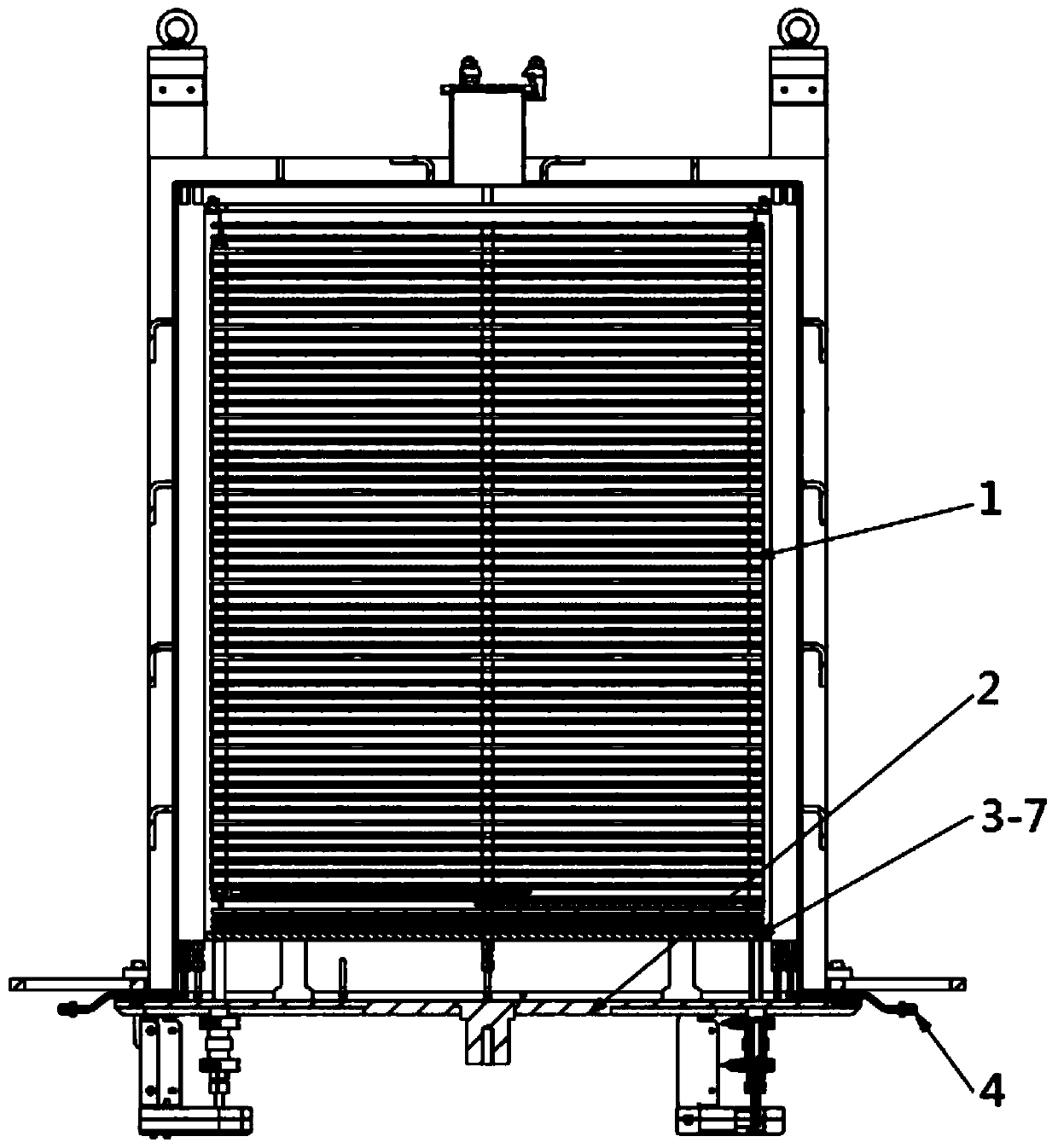
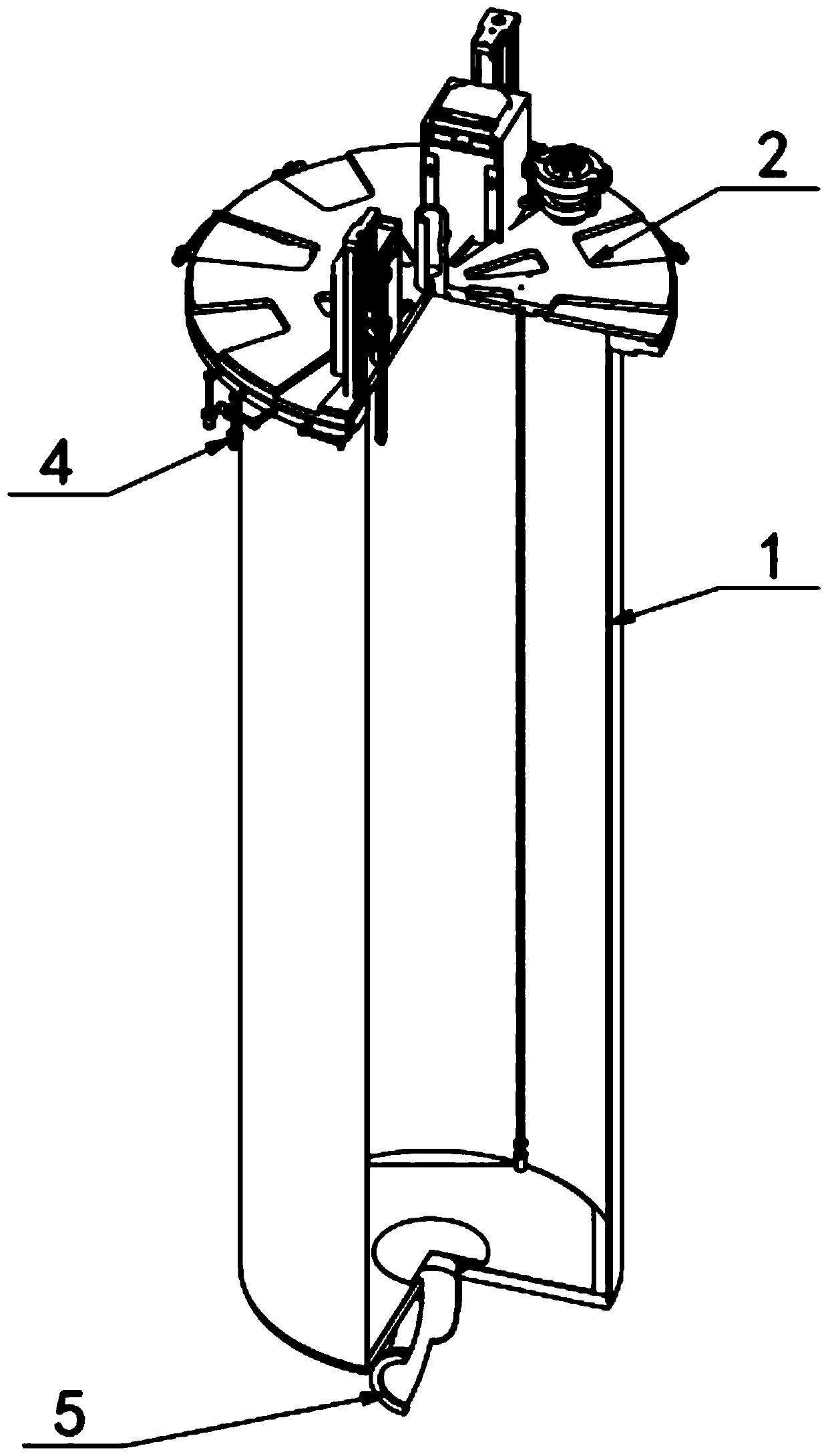
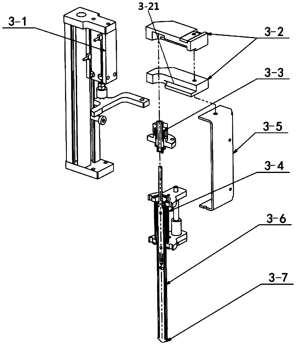
[0035] like Figure 1 to Figure 6 As shown, the semiconductor or photovoltaic material processing equipment includes a furnace body 1, a furnace door 2, and an electrode structure is arranged on the furnace door 2. The electrode structure includes an electrode column 3-7, an electrode body 3-5 and insulating materials. The electrode column 3-7 is connected with the electrode main body 3-5, and the insulating material covers the side of the electrode column 3-7. By insulating and covering the electrode columns, only two ends of the electrode columns 3-7 are exposed. It will be more convenient when the furnace door 2 is connected to the electrode structure in the graphite boat, and it will be easier to form a uniform electric field and realize plasma-enhanced chemical vapor phase. deposition. like figure 1 As shown, the graphite boat will be placed in parallel in the furnace body 1, and the silicon wafers on the graphite boat will also be placed in parallel. This placement st...


PUM


Abstract

The invention discloses machining equipment of a semiconductor or a photovoltaic material. The machining equipment comprises a furnace body and a furnace door; an electrode structure is arranged on the furnace door, an adjusting device is arranged on the furnace door and comprises an arc contact surface and a support block; the arc contact surface is arranged between the support block and the furnace door, and a structure matched with the arc contact surface is arranged at a corresponding location of the support block or the furnace body. The invention provides the machining equipment of the semiconductor or photovoltaic material, and the machining equipment is simple in structure, reasonable in electrode mechanism design, capable of realizing longitudinal arrangement of a graphite boat piece due to the perfect combination of the furnace door, and capable of quickly adjusting the furnace door to reach good sealing effect.

Description

technical field [0001] The invention relates to the field of semiconductor or photovoltaic material processing, more specifically, it relates to a semiconductor or photovoltaic material processing equipment. Background technique [0002] Semiconductor or photovoltaic materials are widely used in electronics, new energy and other industries. Semiconductor and photovoltaic materials usually require chemical treatment before they can be applied to products. CVD technology is one of the processing methods. CVD is chemical vapor deposition. CVD technology is currently It has been widely used in the processing of semiconductor or photovoltaic materials. Common processing equipment includes PECVD, LPCVD, APCVD, etc. In addition to CVD, there are also diffusion processes, such as phosphorus diffusion, boron diffusion, etc., which can use gas diffusion to treat raw materials. Processing. At present, there are many related equipment in the industry. The corresponding equipment can be ...

Claims


Application Information

Patent Timeline
IPC IPC(8): H01L21/67H01L21/02H01L21/383H01L31/18
CPCH01L21/67098H01L21/0262H01L21/383H01L31/1876Y02E10/50Y02P70/50
Inventor 刘群徐栋林佳继朱太荣林依婷
Owner LAPLACE RENEWABLE ENERGY TECH CO LTD
Why Eureka
Try Eureka