Superposed battery structure of perovskite and N-type silicon-based back contact battery
A back contact battery and perovskite technology, applied in the field of solar cells, can solve the problems of battery current output loss, poor PN junction quality, uneven square resistance, etc., and achieve the effect of realizing output and improving photoelectric conversion efficiency
- Summary
- Abstract
- Description
- Claims
- Application Information
AI Technical Summary
Problems solved by technology
Method used
Image
Examples
Embodiment
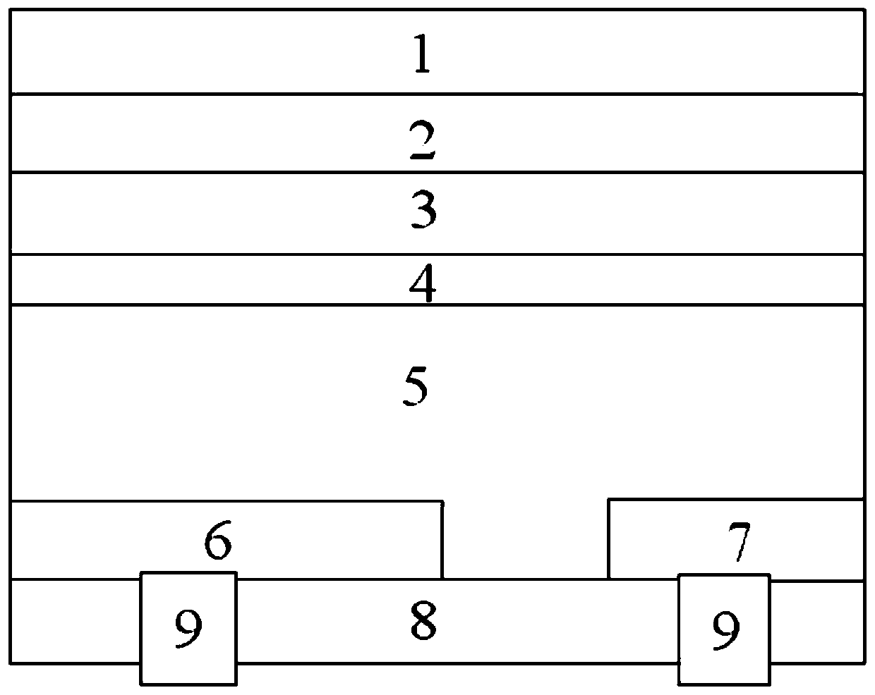
[0014] Such as figure 1 As shown, a perovskite and N-type silicon-based back contact battery stacked battery structure provided by the present invention is characterized in that it includes: a perovskite material absorption layer 1, a front transparent conductive film deposition layer 2, a front passivation layer layer 3, front surface field 4, N-type single crystal silicon wafer substrate 5 and back passivation layer 8, between the N-type single crystal silicon wafer substrate 5 and the back passivation layer 8 are provided with mutually independent rear P+ doped The impurity layer 6 and the back N+ doped layer 7, two metal electrodes. 9 is respectively connected to the rear P+ doped layer 6 and the rear N+ doped layer 7, and is exposed from the surface of the rear passivation layer 8.
[0015] Both the front passivation layer 3 and the back passivation layer 8 are SiO 2 layer; the front transparent conductive film deposition layer 2 is an ITO conductive film layer.
[001...
PUM
 Abstract
Description
Claims
Application Information
