

Vertical cavity surface emitting laser and preparation method thereof
A technology of vertical cavity surface emission and lasers, which is applied in the direction of lasers, laser components, semiconductor lasers, etc., can solve the problems of low production efficiency, long VCSEL production cycle, and high production cost, so as to reduce the production cycle, high reflectivity, reduce The effect of the preparation process
- Summary
- Abstract
- Description
- Claims
- Application Information
AI Technical Summary
Problems solved by technology
Method used
Image

Examples
preparation example Construction
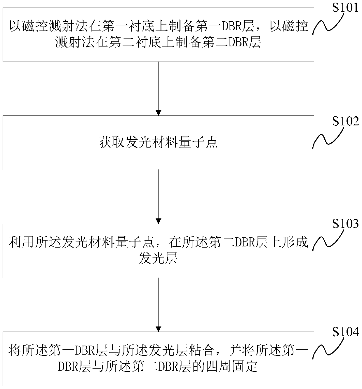
[0056] In view of this, an embodiment of the present application provides a method for manufacturing a vertical cavity surface emitting laser, and the method for manufacturing a vertical cavity surface emitting laser includes:
[0057] Prepare the first DBR layer on the first substrate by magnetron sputtering, and prepare the second DBR layer on the second substrate by magnetron sputtering;
[0058] Obtain quantum dots of luminescent materials;
[0059] forming a luminescent layer on the second DBR layer by using the luminescent material quantum dots;
[0060] The first DBR layer is bonded to the light-emitting layer, and the first DBR layer is fixed to the periphery of the second DBR layer.
[0061] The preparation method of the vertical cavity surface emitting laser is to form the first DBR layer and the second DBR layer on the first substrate and the second substrate respectively by the magnetron sputtering method, and by using quantum dots of luminescent materials, on the...
PUM
| Property | Measurement | Unit |
|---|---|---|
| refractive index | aaaaa | aaaaa |
| refractive index | aaaaa | aaaaa |
Abstract
Description
Claims
Application Information