Novel semiconductor field-effect positive feedback transistor based on bulk silicon substrate and method thereof

A bulk silicon substrate and semiconductor technology, which is applied in the manufacture of transistors, semiconductor devices, semiconductor/solid-state devices, etc., can solve problems such as high price, increased process difficulty and cost, and incompatibility of bulk silicon materials, achieving low process difficulty, The effect of low process cost and high price

Active Publication Date: 2019-12-31
FUDAN UNIV
View PDF5 Cites 2 Cited by
  • Summary
  • Abstract
  • Description
  • Claims
  • Application Information

AI Technical Summary

Problems solved by technology

[0003] However, the aforementioned Z 2 -FETs must be built on a special SOI substrate, which is expensive and incompatible with the bulk silicon material used in large quantities in the industry
Furthermore, to generate the special band structure required for positive feedback, Z 2 -FET has an asymmetric physical structure, which makes it incompatible with the symmetrical structure and self-alignment process of ordinary MOSFETs, and is more susceptible to lithographic alignment errors
This further increases the difficulty and cost of the process

Method used


Image

  • Novel semiconductor field-effect positive feedback transistor based on bulk silicon substrate and method thereof
  • Novel semiconductor field-effect positive feedback transistor based on bulk silicon substrate and method thereof
  • Novel semiconductor field-effect positive feedback transistor based on bulk silicon substrate and method thereof

Examples


Embodiment 1

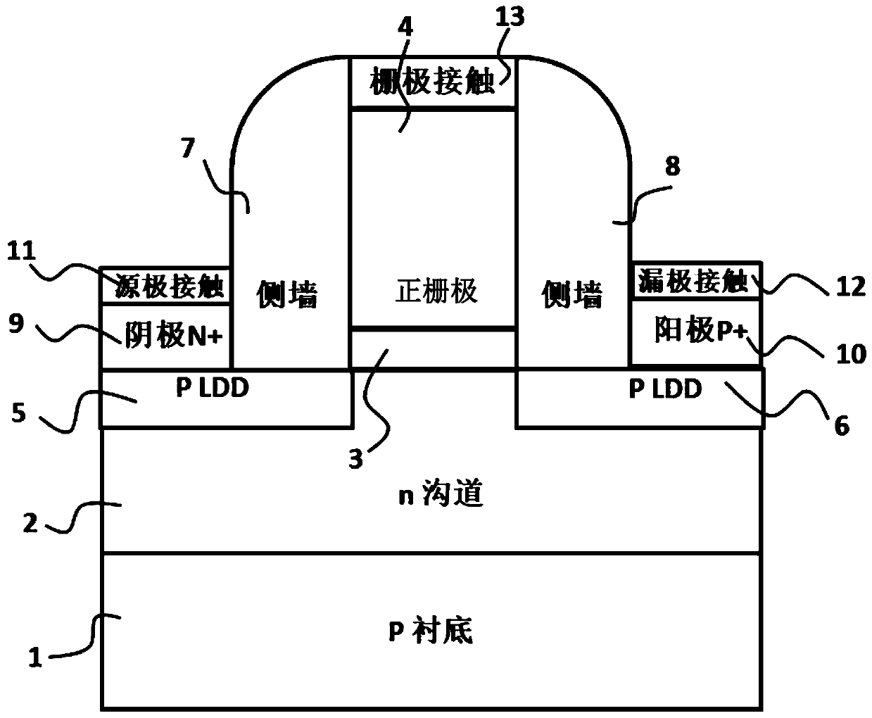
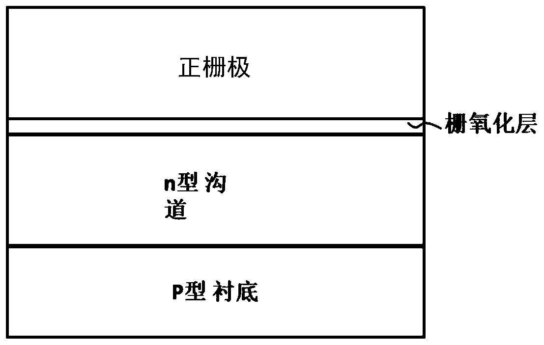
[0053] Such as figure 1 As shown, the novel semiconductor field effect positive feedback transistor based on a bulk silicon substrate of the present invention includes a substrate 1, an epitaxial channel layer 2, a gate oxide layer 3 covering the channel layer, and a positive gate 4 arranged sequentially from bottom to top; Specifically, the channel layer 2 is located on the substrate 1 , the gate oxide layer 3 is located on the channel layer 2 , and the positive gate 4 is located on the gate oxide layer 3 .

[0054] The substrate 1 is undoped or weakly doped, and the substrate 1 and the channel layer 2 are inversely doped, that is, one side is n-type doped while the other side is p-type doped. In the first embodiment, the substrate 1 is weakly p-type doped, and the channel layer 2 is n-type doped.

[0055] A low-drain doped region 5 (LDD) and a low-drain doped region 6 (LDD) are respectively provided on both sides of the positive gate 4, and both the low-drain doped region 5...

Embodiment 2

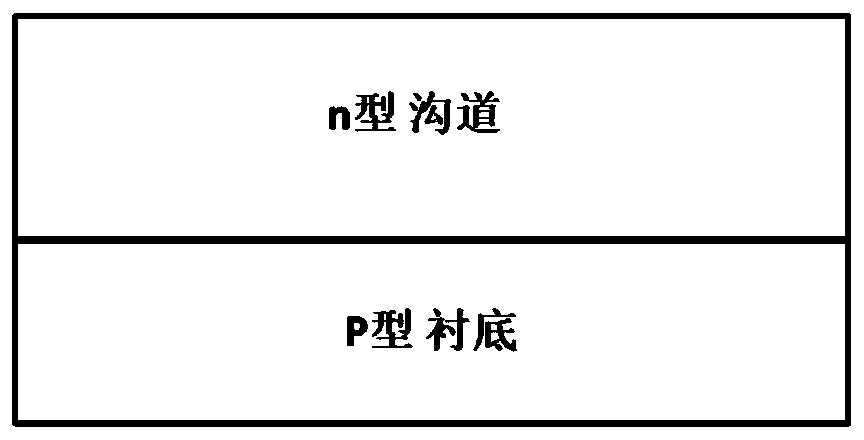
[0081] Such as figure 2 As shown, the device structure and method of Embodiment 2 are similar to Embodiment 1, the difference is that Embodiment 2 is a p-type device, while Embodiment 1 is an n-type device. Specifically: the substrate 1 in the second embodiment is n-type doped, the low-drain doped region 5 and the low-drain doped region 6 are both n-type doped, and the channel layer 2 is p-type doped.

[0082] The realization of the structure of the second embodiment only needs to replace the substrate 1 with n-type doping, the channel layer 2 with p-type doping, and the ion implantation of LDD with n-type on the basis of the first embodiment. Specifically: the substrate doping is weak n-type doping, and the doping concentration is 10 15 cm -2 to 10 19 cm -2 between. On the original silicon wafer, a p-type doped channel layer is epitaxially, and its doping concentration is 10 15 cm -2 to 10 19 cm -2 Between, and the thickness is between 50nm and 1000nm. In addition,...

Embodiment 3

[0084] Such as image 3 As shown, the device structure and method of the third embodiment are similar to the structure of the first embodiment, the difference lies in the formation of the cathode and anode regions. Among them, in the third embodiment, the epitaxy of the cathode region 9 and the anode region 10 does not require in-situ doping, nor does it require a mask; after the epitaxy, combined with photolithography and ion implantation, selectively Form the doping of n+ and p+; the specific steps are similar to the first embodiment, the difference is that step S6 and step S7 are replaced by the following steps: an epitaxial silicon layer with a thickness between 10nm and 100nm; Open the cathode area engraved, inject arsenic or phosphorus, the dose is 10 14 cm -2 to 10 16 cm -2 The energy is between 1keV and 10keV; the anode area is opened by photolithography, and boron or BF2 is implanted with a dose of 10 14 cm -2 to 10 16 cm -2 Between, the energy is between 1keV...


PUM


Abstract

The invention discloses a novel semiconductor field-effect positive feedback transistor based on a bulk silicon substrate and a method thereof. Source and drain electrodes of the transistor are in reverse heavy doping, wherein one side is in p<+> type doping, and the other side is in n<+> type doping; a channel is in weak doping; a low-drain doped region (LDD) defined by grid side walls is close to the channel; and the substrate is doped opposite to the channel in doping type. A traditional field-effect positive feedback device, such as a Z<2>-FET, is established on a silicon-on-insulator (SOI) substrate, so that the traditional field-effect positive feedback device is high in price and asymmetric in structure and is incompatible with a common bulk silicon CMOS process and a device structure; and by introducing the key LDD, channel and substrate doping, the structure-symmetry novel semiconductor field-effect positive feedback transistor is formed on the bulk silicon substrate. The novel device provided by the invention is lower in process cost and smaller in process difficulty, and can be widely applied to the fields of high-performance dynamic and static memories (DRAM and SRAM),low sub-threshold swing switches and electrostatic protection and sensing and the like.

Description

technical field [0001] The invention relates to the technical field of semiconductor devices, in particular to a novel semiconductor field-effect positive-feedback transistor based on a bulk silicon substrate and a preparation method thereof. Background technique [0002] In 2011, the existing technology disclosed a new type of semiconductor device with a completely different working mechanism from ordinary MOSFETs, Z 2 -FET (references: J.Wan, C.Le Royer, A.Zaslavsky and S. Cristoloveanu, Z2-FET field-effect transistor with a vertical subthreshold slope and with no impactization, 2013, U.S. Patent: US8,581,310; and reference Literature: J. Wan, S. Cristoloveanu, C. LeRoyer and A. Zaslavsky, Dynamic memory cell provided with a field-effect transistor having zero swing, 2013, US Patent: 20,130,100,729). Z 2 -FET is built on a silicon-on-insulator (SOI) substrate, and a unique energy band structure is formed in the substrate by introducing an asymmetric device structure and ...

Claims


Application Information

Patent Timeline
Patent Type & Authority Applications(China)
IPC IPC(8): H01L29/78H01L29/08H01L29/10H01L29/16H01L21/336
CPCH01L29/0847H01L29/1033H01L29/1079H01L29/16H01L29/66568H01L29/7833
Inventor 万景
Owner FUDAN UNIV
Why Eureka
Try Eureka