Silicon carbide MOSFET power device and preparation method thereof
A technology of power devices and silicon carbide, which is applied in the manufacture of semiconductor/solid-state devices, semiconductor devices, electrical components, etc., can solve the problems of large on-resistance of devices, large electric field strength in gate oxide, etc., and achieves remarkable effects, device structure and The effect of simple preparation process and wide application prospect
- Summary
- Abstract
- Description
- Claims
- Application Information
AI Technical Summary
Problems solved by technology
Method used
Image
Examples
Embodiment 1
[0077] See Figure 1 to Figure 14 . It should be noted that the illustrations provided in this embodiment only illustrate the basic idea of the present invention in a schematic manner, although the illustrations only show the components related to the present invention instead of the actual implementation of the number, shape and For size drawing, the shape, quantity, and proportion of each component can be changed at will during actual implementation, and the component layout may be more complicated.
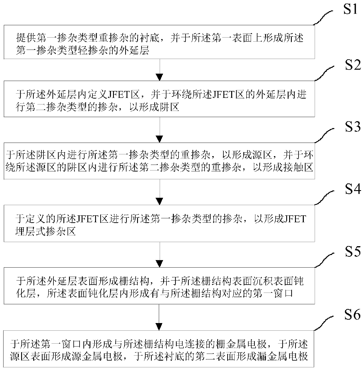
[0078] Such as Figure 1 to Figure 14 As shown, the present invention provides a method for manufacturing a silicon carbide MOSFET power device, including the following steps:
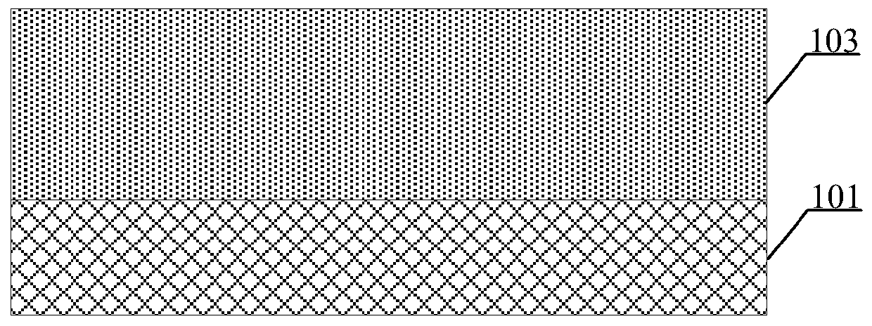
[0079] S1: providing a heavily doped substrate of the first doping type, and the substrate has a first surface and a second surface, and forming a lightly doped epitaxial layer of the first doping type on the first surface;
[0080] S2: Define a JFET region in the epitaxial layer, and perform doping of the ...
Embodiment 2
[0144] See Figure 1 to Figure 14 . It should be noted that the illustrations provided in this embodiment only illustrate the basic idea of the present invention in a schematic manner, although the illustrations only show the components related to the present invention instead of the actual implementation of the number, shape and For size drawing, the shape, quantity, and proportion of each component can be changed at will during actual implementation, and its component layout may also be more complicated.
[0145] Such as Figure 1 to Figure 14 As shown, the present invention provides a method for manufacturing a silicon carbide MOSFET power device, including the following steps:
[0146] S1: providing a heavily doped substrate of the first doping type, and the substrate has a first surface and a second surface, and forming a lightly doped epitaxial layer of the first doping type on the first surface;
[0147] S2: Define a JFET region in the epitaxial layer, and perform doping of...
Embodiment 3
[0211] See Figure 1 to Figure 14 . It should be noted that the illustrations provided in this embodiment only illustrate the basic idea of the present invention in a schematic manner, although the illustrations only show the components related to the present invention instead of the actual implementation of the number, shape and For size drawing, the shape, quantity, and proportion of each component can be changed at will during actual implementation, and the component layout may be more complicated.
[0212] Such as Figure 1 to Figure 14 As shown, the present invention provides a method for manufacturing a silicon carbide MOSFET power device, including the following steps:
[0213] S1: providing a heavily doped substrate of the first doping type, and the substrate has a first surface and a second surface, and forming a lightly doped epitaxial layer of the first doping type on the first surface;
[0214] S2: Define a JFET region in the epitaxial layer, and perform doping of the ...
PUM
| Property | Measurement | Unit |
|---|---|---|
| Thickness | aaaaa | aaaaa |
| Thickness | aaaaa | aaaaa |
| Thickness | aaaaa | aaaaa |
Abstract
Description
Claims
Application Information
 - R&D
- Intellectual Property
- Life Sciences
- Materials
- Tech Scout
- Unparalleled Data Quality
- Higher Quality Content
- 60% Fewer Hallucinations
Browse by: Latest US Patents, China's latest patents, Technical Efficacy Thesaurus, Application Domain, Technology Topic, Popular Technical Reports.
© 2025 PatSnap. All rights reserved.Legal|Privacy policy|Modern Slavery Act Transparency Statement|Sitemap|About US| Contact US: help@patsnap.com


