A method for large-area monolayer graphene preparation using metal intercalation

A single-layer graphene, large-area technology, applied in the direction of single-layer graphene, graphene, nano-carbon, etc., can solve the problems of difficult to control layer thickness, many defects, etc., achieve low temperature dependence, simple preparation conditions, repeatable good sex effect

Active Publication Date: 2021-07-13
XI AN JIAOTONG UNIV
View PDF6 Cites 0 Cited by
  • Summary
  • Abstract
  • Description
  • Claims
  • Application Information

AI Technical Summary

Problems solved by technology

[0005] The purpose of the present invention is to solve the problem that the method for preparing graphene by metal intercalation has many defects and is difficult to control its layer thickness in the prior art, and provides a method for preparing single-layer graphene by using metal intercalation in a large area

Method used


Image

  • A method for large-area monolayer graphene preparation using metal intercalation
  • A method for large-area monolayer graphene preparation using metal intercalation
  • A method for large-area monolayer graphene preparation using metal intercalation

Examples


Embodiment 1

[0044] 1) A grade A single crystal 6H-SiC (0001) substrate with a size of 15mm×3mm×330μm was selected as the growth substrate of epitaxial graphene;

[0045] 2) Place the single crystal SiC substrate in a vacuum preparation chamber and heat it to 820K for degassing. The pressure of the vacuum preparation chamber is maintained at 5×10 -10 Torr, the DC power used is 0.5A, and the water vapor and residue adsorbed on the surface of the single crystal SiC are removed after 8 hours of degassing;

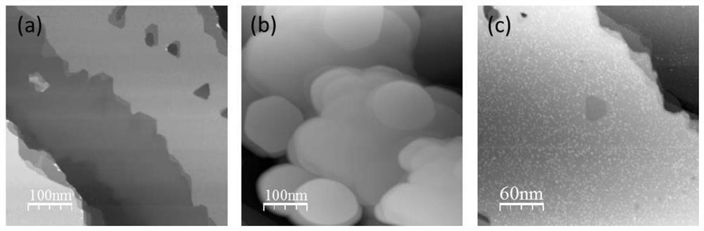
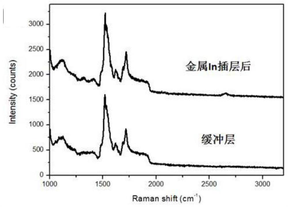
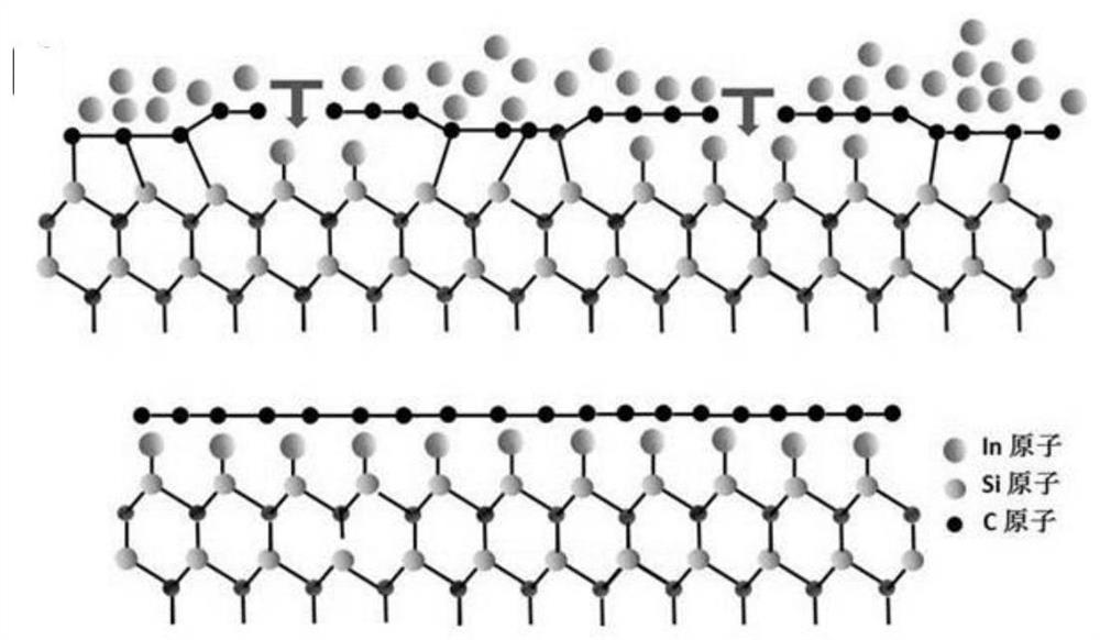
[0046] 3) Raise the temperature of the single crystal SiC substrate obtained in step 2) to 1470K and keep it for 15 minutes, so that a large-area buffer layer is formed on the surface of SiC, and the morphology of the single crystal SiC surface covered by the buffer layer is as follows: figure 1 as shown in (a);

[0047] 4) heating the metal In source in the crucible K~Cell device;

[0048] 5) Maintain the temperature of the single crystal SiC substrate at 80K, open the baffle of the met...

Embodiment 2

[0053] 1) A grade A single crystal 6H-SiC (0001) substrate with a size of 15mm×3mm×330μm was selected as the growth substrate of epitaxial graphene;

[0054] 2) Place the single crystal SiC substrate in a vacuum preparation chamber and heat to 800K to degas, and the pressure of the vacuum preparation chamber is maintained at 5×10 -10 Torr, the DC power used is 0.48A, and after 8 hours of degassing, the water vapor and residue adsorbed on the surface of the single crystal SiC are removed;

[0055] 3) Raise the temperature of the single crystal SiC substrate obtained in step 2) to 1620K and keep it for 5 minutes, so that the SiC surface forms a buffer layer and the single-layer epitaxial graphene coexists on the surface, and the surface of the single crystal SiC covered by the buffer layer and epitaxial graphene looks like Figure 4 as shown in (a);

[0056] 4) heating the metal In source in the crucible K~Cell device;

[0057] 5) Maintain the temperature of the single crysta...

Embodiment 3

[0062] 1) A grade A single crystal 6H-SiC (0001) substrate with a size of 15mm×3mm×330μm was selected as the growth substrate of epitaxial graphene;

[0063] 2) Place the single crystal SiC substrate in a vacuum preparation chamber and heat it to 840K for outgassing. The pressure of the vacuum preparation chamber is maintained at 5×10 -10 Torr, the DC power used is 0.52A, and the water vapor and residue adsorbed on the surface of the single crystal SiC are removed after 8 hours of degassing;

[0064] 3) heating the single crystal SiC substrate obtained in step 2) to 1470K and keeping it for 12 minutes, so that a large-area buffer layer is formed on the SiC surface;

[0065] 4) heating the metal In source in the crucible K~Cell device;

[0066] 5) Maintain the temperature of the single crystal SiC substrate at 80K, open the baffle of the metal beam source, and deposit metal In atoms. During the deposition process, the heating current of the metal In source is 2.8A, the heating...


PUM


Abstract

The invention discloses a large-area single-layer graphene preparation technology. The buffer layer is intercalated with In atoms by using the intercalation technology. Originally, only the surface of the buffer layer is used, and the In atoms are inserted between the buffer layer and the SiC substrate to make the buffer layer Converting to graphene, on the one hand, a single layer of large-area graphene is prepared, and on the other hand, the preparation temperature of graphene is reduced. On the surface where the original buffer layer and single-layer epitaxial graphene coexist, In atoms are inserted between the buffer layer and the SiC substrate, the buffer layer becomes graphene and is perfectly connected with the original epitaxial graphene, forming a large-area single-layer graphene . In addition, the intercalation-formed graphene has a weak interaction with the substrate, and it is separated graphene, which achieves the effect of ionization. This technology can not only prepare large-area graphene, but also control the layer thickness of graphene, which provides important guidance and reference value for applications in related fields such as microelectronics, superconductivity, and strain engineering.

Description

【Technical field】 [0001] The invention belongs to the field of two-dimensional material preparation and modification, and relates to a method for preparing single-layer graphene in a large area by metal intercalation. 【Background technique】 [0002] The invention of silicon-based integrated circuits has accelerated the informatization process of human society. However, with the advancement of technology, the feature size of devices tends to be at the nanometer level. It is difficult to effectively manufacture products with stable electrical properties and higher integration due to the influence of microscopic physical effects. Therefore, the exploration of new technologies or new materials has become urgent. Graphene is a two-dimensional system material. Because of its small size, controllable shape and fast electron movement speed (up to 1 / 300 of the speed of light), it has become a new material that may replace traditional silicon. Graphene has broad application prospects...

Claims


Application Information

Patent Timeline
Patent Type & Authority Patents(China)
IPC IPC(8): C01B32/188
CPCC01B2204/02C01B32/188
Inventor 惠欣胡廷伟杨东马飞马大衍徐可为
Owner XI AN JIAOTONG UNIV
Why Eureka
Try Eureka