Hyperbolic metamaterial planar antenna
A technology of planar antenna and curved super, applied in the field of planar antenna, can solve the problems of thin film antenna dielectric substrate, complex design of electromagnetic bandgap antenna, not easy to process, etc., to achieve increased gain, excellent anti-interference ability, and easy production and processing Effect
- Summary
- Abstract
- Description
- Claims
- Application Information
AI Technical Summary
Problems solved by technology
Method used
Image
Examples
Embodiment 1
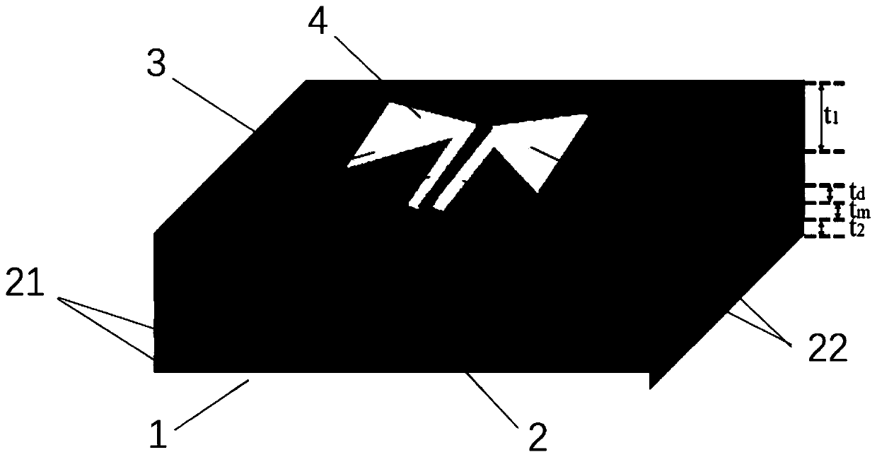
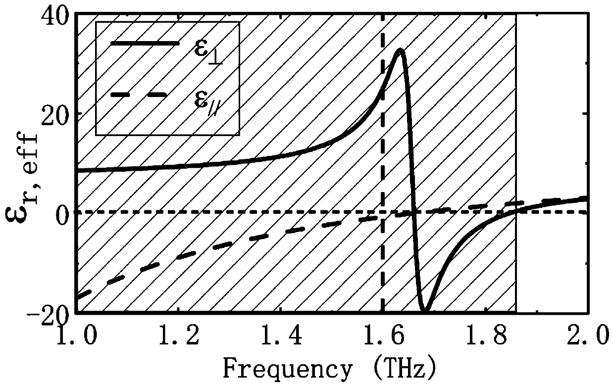
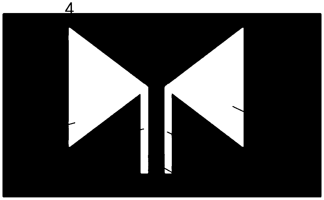
[0040] The hyperbolic metamaterial terahertz planar antenna involved in this embodiment has a three-dimensional structure as attached figure 1 shown. Its overall structure includes a ground plane 1 , a hyperbolic metamaterial structure layer 2 , a substrate 3 , and a radiation antenna 4 . The ground plate 1 is a metal layer made of gold with a uniform thickness, and its thickness is t 2 = 200nm. The hyperbolic metamaterial structure layer 2 is formed by alternate stacking of semiconductor layers 21 and dielectric layers 22 , the semiconductor layers 21 are formed of indium antimonide material, and the dielectric constant thereof can be calculated by the Drude model. The real part of the dielectric constant of the indium antimonide material is negative within a certain range of terahertz frequencies, and the imaginary part is small, so it meets the design requirements of hyperbolic metamaterials, and the loss generated in the terahertz band is also small. The dielectric laye...
Embodiment 2
[0050] On the basis of the antenna described in Embodiment 1, only the total number of layers of the hyperbolic metamaterial structure layer 2 is changed. In this embodiment, the total number of layers of the hyperbolic metamaterial structure layer 2 is 6, that is, a semiconductor layer 21 is first formed on the ground plate 1, and a dielectric layer is formed on the semiconductor material layer 21. twenty two. Sequentially, the semiconductor layer 21 and the dielectric layer 22 are alternately formed until the hyperbolic metamaterial structure layer 2 with a total of 6 layers is formed.
[0051] attached Figure 5 shown, with Figure 5 The dark solid lines (Reference) shown in (a) and (b) are based on the structure described in Example 1, and the other structure dimensions are not changed, and the terahertz frequency without using the hyperbolic metamaterial structure layer The echo curve and antenna pattern of the planar antenna are used as reference curves for comparison...
Embodiment 3
[0054] On the basis of the antenna described in Embodiment 1, only the total number of layers of the hyperbolic metamaterial structure layer 2 is changed. In this embodiment, the total number of layers of the hyperbolic metamaterial structure layer 2 is 8, that is, a semiconductor layer 21 is first formed on the ground plate 1, and a dielectric layer is formed on the semiconductor material layer 21. 22. Alternately reciprocate until a hyperbolic metamaterial structure layer 2 with a total of 8 layers is formed.
[0055] attached Figure 5 (a) The light-colored dotted line (8layers) is the echo curve of the hyperbolic metamaterial terahertz planar antenna in this embodiment. It can be seen from the figure that the operating frequency bandwidth of the antenna is 1.08THz~1.14THz. The working center frequency is 1.11THz. attached Figure 5 The light-colored dashed line (8layers) in (b) is the antenna pattern of the hyperbolic metamaterial terahertz planar antenna in this embodi...
PUM
| Property | Measurement | Unit |
|---|---|---|
| Thickness | aaaaa | aaaaa |
| Resonance frequency | aaaaa | aaaaa |
| Thickness | aaaaa | aaaaa |
Abstract
Description
Claims
Application Information


