Tunneling field effect transistor and forming method thereof

A tunneling field effect, transistor technology, applied in the manufacturing of diodes, semiconductor devices, semiconductor/solid-state devices, etc., can solve the problems of poor driving ability, low threshold slope, low operating voltage, etc., to achieve good conductivity and reduce contact resistance. , the effect of increasing the current

Pending Publication Date: 2020-01-21
SEMICON MFG INT (SHANGHAI) CORP +1
View PDF0 Cites 0 Cited by
  • Summary
  • Abstract
  • Description
  • Claims
  • Application Information

AI Technical Summary

Problems solved by technology

[0004] TFET has many excellent characteristics such as low leakage current, low threshold slope, low operating v

Method used


Image

  • Tunneling field effect transistor and forming method thereof
  • Tunneling field effect transistor and forming method thereof
  • Tunneling field effect transistor and forming method thereof

Examples


Example Embodiment

[0031] As described in the background art, the tunneling field effect transistor of the prior art has poor performance.

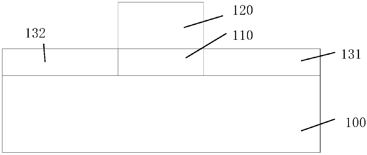
[0032] figure 1 It is a schematic diagram of the structure of a tunneling field effect transistor.

[0033] A tunneling field effect transistor, reference figure 1 , Including: a semiconductor substrate 100, a channel region 110 on the surface of the semiconductor substrate 100, a gate structure 120 on the surface of the channel region, and a third doped region in the semiconductor substrate 100 on both sides of the gate structure 120 131 and the fourth doped region 132.

[0034] The third doped region 131 and the fourth doped region 132 are the source terminal and the drain terminal of the tunneling field effect transistor, respectively, one of which is a P region (hole doping) and the other is an N region (electron doping) ), the middle channel region 110 is an intrinsic material. Under the driving voltage, holes can tunnel from the P region to the N region to...


PUM

PropertyMeasurementUnit
Thicknessaaaaaaaaaa
Thicknessaaaaaaaaaa

Abstract

The invention discloses a tunneling field effect transistor and a forming method thereof. The method comprises the steps that a semiconductor substrate is provided, a channel region is arranged in thesemiconductor substrate, a gate structure is arranged on a surface of the channel region, a first silicide layer and a second silicide layer are formed in the semiconductor substrate on two sides ofthe gate structure, and a distance between the first silicide layer and a side wall of the gate structure and the distance between the second silicide layer and the side wall of the gate structure aregreater than zero; a first doped region is formed between the first silicide layer and the gate structure, wherein the first doped region has first ions; and a second doped region is formed between the second silicide layer and the gate structure, the second doped region has second ions, and the first ions and the second ions are opposite in conductivity type. By using the method, performance ofa tunneling field effect transistor is improved.

Description

technical field [0001] The invention relates to the field of semiconductor manufacturing, in particular to a tunneling field effect transistor and a forming method thereof. Background technique [0002] With the rapid development of semiconductor manufacturing technology, semiconductor devices are developing towards higher component density and higher integration, and the feature size of CMOS devices, which are the core semiconductor devices, is constantly shrinking. Subsequently, the negative effects such as the short channel effect of the device become more and more serious. Effects such as leakage-induced barrier reduction and band-band tunneling increase the off-state leakage current of the device. At the same time, the subthreshold slope of the traditional MOSFET is limited by the thermoelectric potential and cannot be reduced synchronously with the shrinking of the device size. increased device power consumption. The power consumption problem has become the most seve...

Claims


Application Information

Patent Timeline
IPC IPC(8): H01L21/331H01L29/739H01L29/45
CPCH01L29/66356H01L29/7391H01L29/456
Inventor 赵猛
Owner SEMICON MFG INT (SHANGHAI) CORP
Why Eureka
Try Eureka