Semiconductor device and formation method thereof

A semiconductor and device technology, applied in the field of semiconductor devices and their formation, can solve the problems of uneven thermal expansion and stress of switch holes, poor sidewall flatness, poor flatness, etc., and achieve uniform thermal expansion and stress, high flatness, and improved stability and performance

Active Publication Date: 2020-01-31
WUHAN XINXIN SEMICON MFG CO LTD
View PDF19 Cites 0 Cited by
  • Summary
  • Abstract
  • Description
  • Claims
  • Application Information

AI Technical Summary

Problems solved by technology

[0004] On the other hand, if figure 2 As shown, the Bosch process is used to form the TSV 004. The Bosch process brings poor side wall flatness, that is, the inner wall (side) of the TSV 004 (switch hole) has poor flatness (such as

Method used


Image

  • Semiconductor device and formation method thereof
  • Semiconductor device and formation method thereof
  • Semiconductor device and formation method thereof

Examples


Embodiment Construction

[0039] The semiconductor device and its forming method proposed by the present invention will be further described in detail below with reference to the accompanying drawings and specific embodiments. The advantages and features of the present invention will become clearer from the following description. It should be noted that all the drawings are in a very simplified form and use imprecise scales, and are only used to facilitate and clearly assist the purpose of illustrating the embodiments of the present invention.

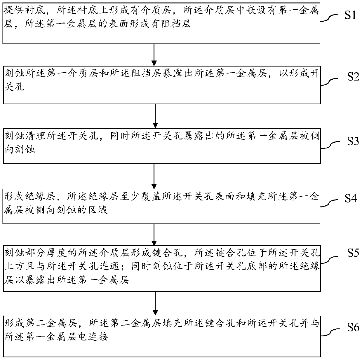
[0040] An embodiment of the present invention provides a method for forming a semiconductor device, such as image 3 shown, including:

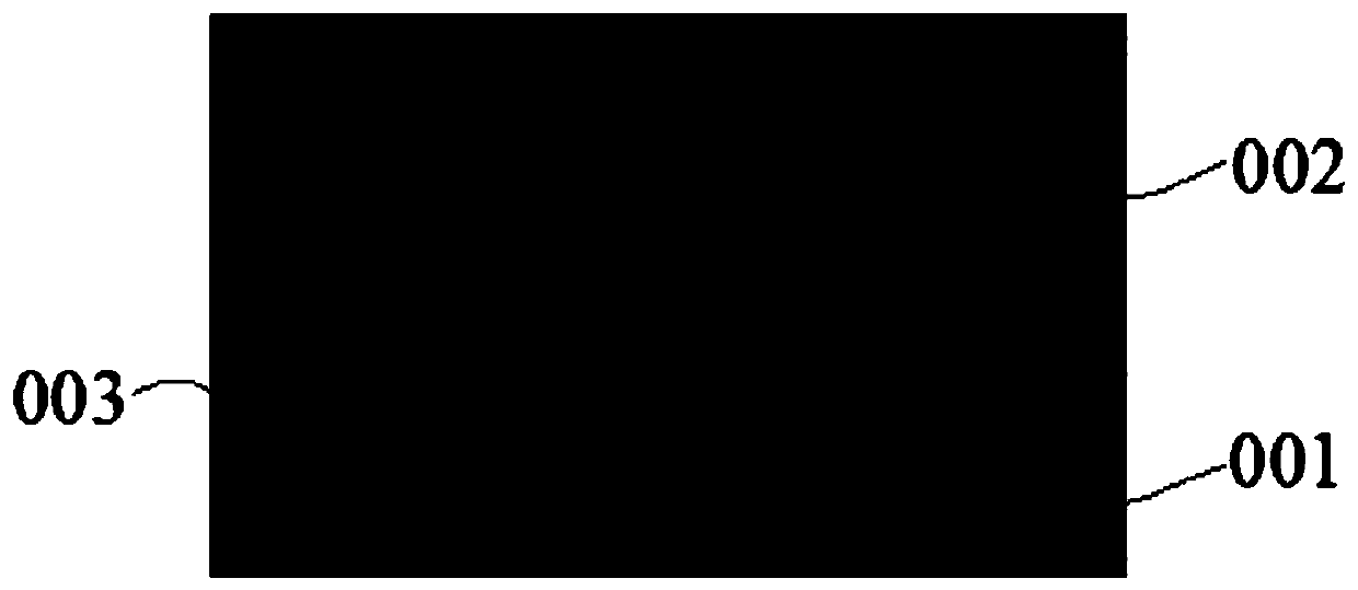
[0041] A substrate is provided, a dielectric layer is formed on the substrate, a first metal layer is embedded in the dielectric layer, and a barrier layer is formed on the surface of the first metal layer;

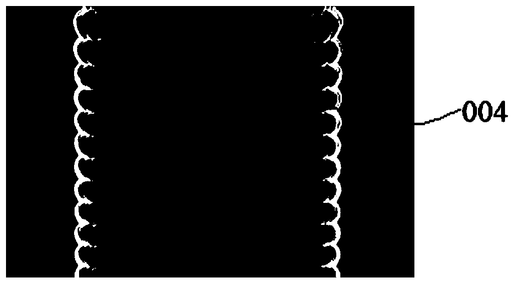
[0042] Etching the first dielectric layer and the barrier layer to expose the first metal layer to form switch holes;...


PUM


Abstract

The invention provides a semiconductor device and a formation method thereof. The formation method comprises the following steps: providing a substrate; etching a first dielectric layer and a barrierlayer to expose a first metal layer so as to form a switch hole; etching and cleaning the switch hole, while the first metal layer exposed out of the switch hole is laterally etched; and forming an insulating layer which at least covers the surface of the switch hole and fills the area where the first metal layer is laterally etched. The area where the first metal layer is laterally etched is filled with the insulating layer, thus avoiding the formation of gaps and improving the stability and the reliability of the contact resistance in the switch hole. The insulating layer of the side wall ofthe switch hole separates the first metal layer of the bottom circumferential ring of the switch hole to prevent it from being damaged, and the insulating layer covers the side wall of the switch hole so that the flatness of the switch hole is high, the uniformity of film deposition in the switch hole and the metal layer filling the switch hole is improved and the thermal expansion and stress areenabled to be uniform.

Description

technical field [0001] The invention belongs to the technical field of integrated circuit manufacturing, and in particular relates to a semiconductor device and a forming method thereof. Background technique [0002] Metal interconnection technology is one of the important technologies in the manufacture of integrated circuits (ICs). Aluminum (Al) is easy to form patterns and has been widely used in the metal wiring of integrated circuits. Copper (Cu) has the characteristics of good electrical conductivity, low resistivity, good resistance to electromigration and stress-free migration. Copper metal layer is deposited on the aluminum metal layer to realize copper electrical connection to aluminum, copper and aluminum are combined and distributed in their respective appropriate positions as the interconnection lines of integrated circuits, taking the advantages of both copper and aluminum, avoiding aluminum Disadvantages such as poor resistance to electromigration and the dis...

Claims


Application Information

Patent Timeline
IPC IPC(8): H01L21/768H01L23/528
CPCH01L21/76805H01L21/76831H01L21/76834H01L21/76882H01L23/5283
Inventor 胡杏叶国梁周玉刘天建
Owner WUHAN XINXIN SEMICON MFG CO LTD
Why Eureka
Try Eureka