Semiconductor epitaxial structure, vcsel and manufacturing method based on flexible substrate

A flexible substrate and epitaxial structure technology, applied in the field of semiconductors, can solve problems such as the difficulty in growing semiconductor epitaxial layers, and achieve the effects of reducing threading dislocations, difficult growth, and good quality

Active Publication Date: 2021-03-09
XIAMEN QIANZHAO SEMICON TECH CO LTD
View PDF8 Cites 0 Cited by
  • Summary
  • Abstract
  • Description
  • Claims
  • Application Information

AI Technical Summary

Problems solved by technology

In the current research, C60 film or metal (such as molybdenum-tungsten-selenium alloy) is only grown on fluorphlogopite, and fluorphlogopite has not been used as a semiconductor epitaxial substrate. The reason is that the semiconductor epitaxial layer is on the fluorphlogopite substrate. difficult to grow

Method used


Image

  • Semiconductor epitaxial structure, vcsel and manufacturing method based on flexible substrate
  • Semiconductor epitaxial structure, vcsel and manufacturing method based on flexible substrate
  • Semiconductor epitaxial structure, vcsel and manufacturing method based on flexible substrate

Examples


Embodiment 1

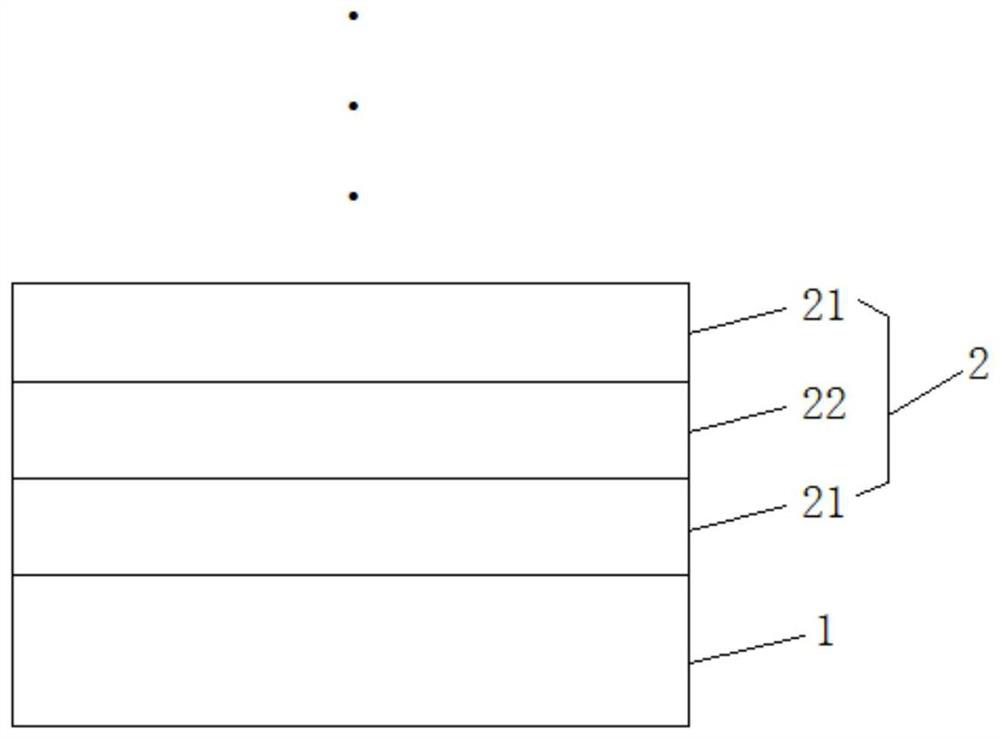
[0070] A semiconductor epitaxial structure based on a flexible substrate, such as Figure 4 As shown, it includes a fluorophlogopite substrate 1 and a buffer layer 2 arranged on the fluorophlogopite substrate 1. The buffer layer 2 includes:

[0071] A multi-layer first GaInP buffer layer 21 and a multi-layer second GaInP buffer layer 22 are provided, and the multi-layer first GaInP buffer layer 21 is sequentially arranged on the fluorophlogopite substrate 1 from bottom to top; two adjacent layers of the first GaInP buffer layer The second GaInP buffer layers 22 are respectively provided between 21 and between the fluorophlogopite substrate 1 and the adjacent first GaInP buffer layers 21 . That is, the second GaInP buffer layer 22 and the first GaInP buffer layer 21 are alternately disposed on the fluorophlogopite substrate 1 from bottom to top.

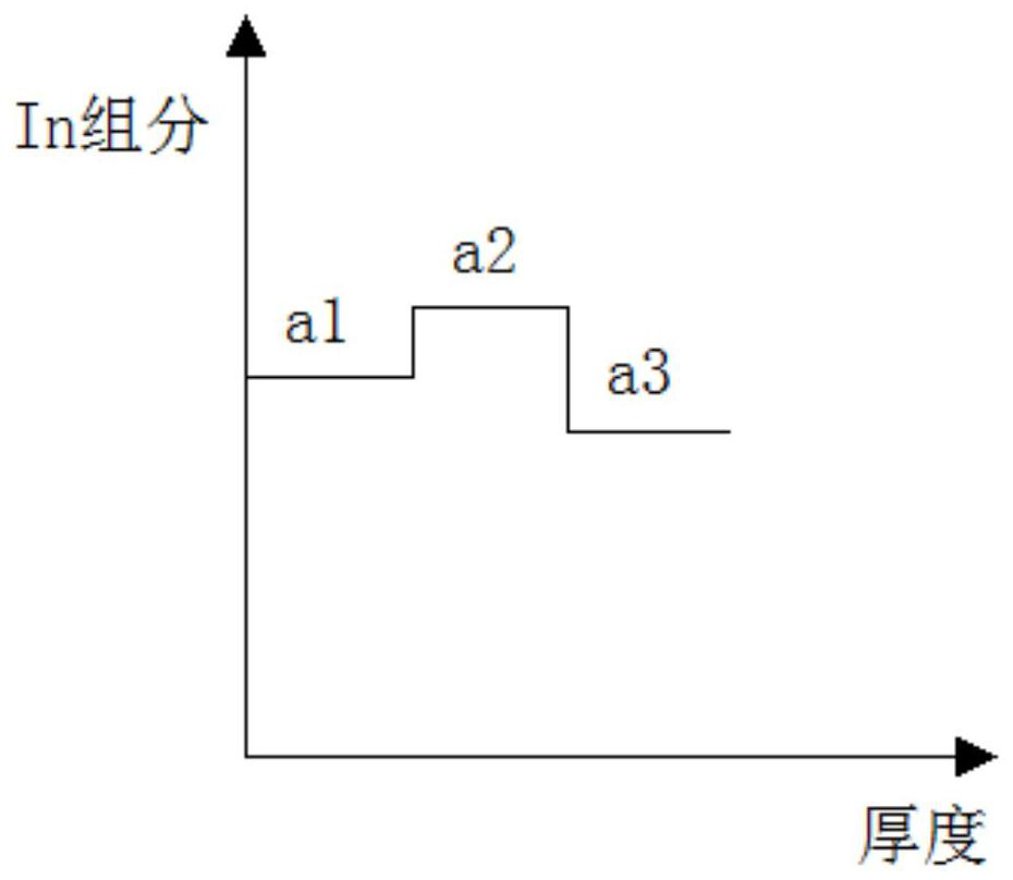
[0072] The In composition of the multilayered first GaInP buffer layer 21 decreases layer by layer from bottom to top, the In compo...

Embodiment 2

[0075] A method for growing a semiconductor epitaxial structure based on a flexible substrate, which is used to fabricate the semiconductor epitaxial structure based on a flexible substrate in the first embodiment, including:

[0076] Provide a fluorophlogopite substrate;

[0077]A buffer layer is grown on the fluorophlogopite substrate, the buffer layer includes a multi-layer first GaInP buffer layer and a multi-layer second GaInP buffer layer, the multi-layer first GaInP buffer layer grows sequentially from bottom to top, and two adjacent The second GaInP buffer layers are respectively provided between the first GaInP buffer layers and between the fluorophlogopite substrate and the adjacent first GaInP buffer layers. Specifically, a buffer layer including multiple layers of the first GaInP buffer layer and multiple layers of the second GaInP buffer layer can be formed by alternately growing the second GaInP buffer layer and the first GaInP buffer layer multiple times on the ...

Embodiment 3

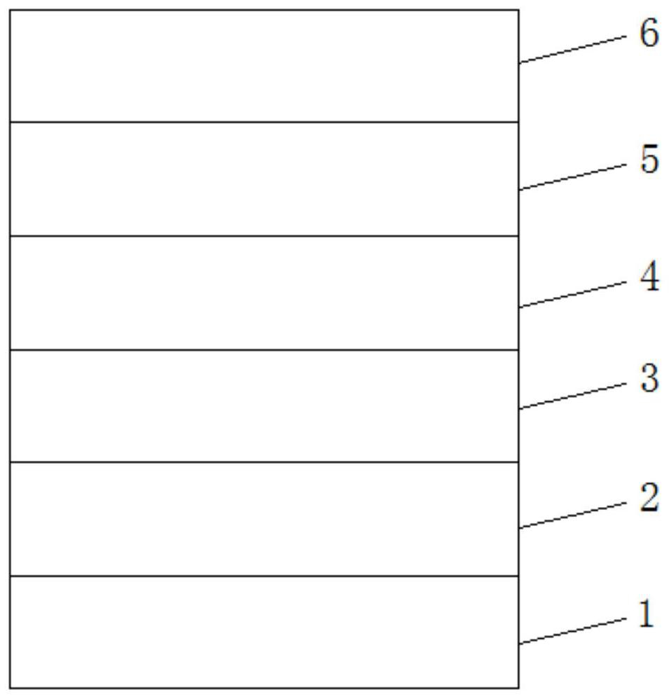
[0079] A VCSEL, comprising the flexible substrate-based semiconductor epitaxial structure described in the first embodiment, and further comprising: an N-type DBR layer 3 sequentially stacked on the buffer layer 2 from bottom to top, a first separation confinement heterogeneity Junction 7, multiple quantum well layer 4, second separation confinement heterojunction 8, oxide layer 5 and P-type DBR layer 6, the schematic diagram is as follows Image 6 shown.


PUM

PropertyMeasurementUnit
thicknessaaaaaaaaaa

Abstract

The invention provides a semiconductor epitaxial structure, VCSEL and manufacturing method based on a flexible substrate. Fluorphlogopite mica is used as the substrate, which not only solves the problem that the existing semiconductor substrate cannot be bent and is not easy to peel off, but also takes into account the cost of the semiconductor device. temperature requirements. For the buffer layer, the multi-layer first GaInP buffer layer is gradually changed layer by layer, showing a step gradient trend. By inserting the second layer of the In composition gradient opposite to the direction of the In composition gradient between two adjacent first GaInP buffer layers. The GaInP buffer layer forms a structure with fluctuating and gradual changes in the In composition, thereby introducing compressive stress in the buffer layer, increasing the interaction of dislocations, making the surface smoother, and further reducing threading dislocations, improving the performance of fluorine phlogopite. The quality of the epitaxial layer on the substrate realizes the application of fluorophlogopite substrate in semiconductor devices. VCSEL has the advantages of being bendable, easy to peel off, good epitaxial layer quality, and high light extraction efficiency.

Description

technical field [0001] The invention relates to the technical field of semiconductors, and in particular, to a semiconductor epitaxial structure based on a flexible substrate, a VCSEL and a manufacturing method. Background technique [0002] VCSEL, the full name of Vertical Cavity Surface Emitting Laser, is developed on the basis of gallium arsenide semiconductor material, which is different from other light sources such as LED (Light Emitting Diode) and LD (Laser Diode, laser diode). Small, circular output light spot, single longitudinal mode output, low threshold current, low price, easy to integrate into a large-area array, etc., are widely used in optical communication, optical interconnection, optical storage and other fields. [0003] Existing VCSELs are usually based on GaAs substrates. However, GaAs substrates limit the application of VCSELs in flexible devices due to their physical properties such as inability to bend, poor mechanical properties, and difficulty in p...

Claims


Application Information

Patent Timeline
Patent Type & Authority Patents(China)
IPC IPC(8): H01S5/02H01S5/183
CPCH01S5/0206H01S5/183
Inventor 李峰柱田宇刘潇杰韩效亚杜石磊
Owner XIAMEN QIANZHAO SEMICON TECH CO LTD
Why Eureka
Try Eureka