Base region ring-doped anti-radiation lateral PNP transistor and preparation method thereof

A base ring and transistor technology, applied in semiconductor/solid-state device manufacturing, semiconductor devices, electrical components, etc., can solve the problems of increased hole diffusion distance, poor ability of lateral PNP transistors to resist total dose radiation, etc., and achieve the purpose of suppressing αT drop, high total dose radiation resistance, reduced effect of β drop

Pending Publication Date: 2020-02-21
XIAN MICROELECTRONICS TECH INST
View PDF5 Cites 3 Cited by
  • Summary
  • Abstract
  • Description
  • Claims
  • Application Information

AI Technical Summary

Problems solved by technology

[0003] The lateral PNP transistor has poor ability to resist total dose radiation: the total dose radiation will cause positive charges to be induced and accumulated in the silicon dioxide layer covering the surface of the transistor, which will induce negative charges on the surface of the transistor, resulting in the P-

Method used


Image

  • Base region ring-doped anti-radiation lateral PNP transistor and preparation method thereof
  • Base region ring-doped anti-radiation lateral PNP transistor and preparation method thereof
  • Base region ring-doped anti-radiation lateral PNP transistor and preparation method thereof

Examples


Embodiment 1

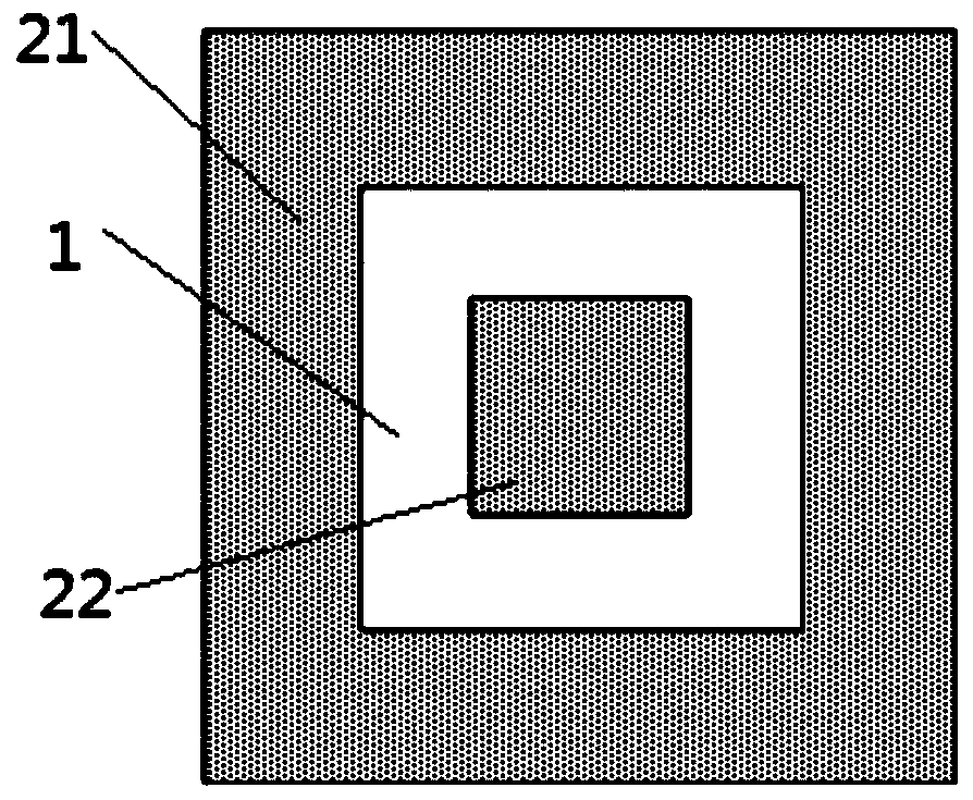
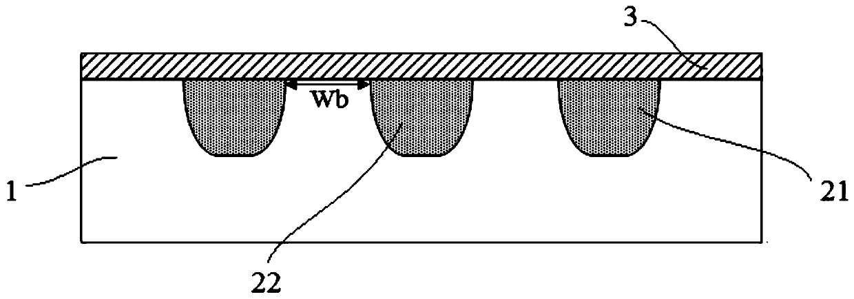
[0044] The N-type base ring lateral PNP transistor structure of the present invention includes an N-type epitaxial layer 1 and a silicon dioxide insulating layer 3 arranged sequentially from bottom to top, and a P-type collector region 21 and a P-type collector region 21 are arranged on the upper part of the N-type epitaxial layer 1. Type emitter region 22, P-type collector region 21 and P-type emitter region 22 are concentrically arranged, and the depth of P-type collector region 21 and P-type emitter region 22 is the same, between P-type collector region 21 and P-type emitter region 22 An N-type base loop 5 is provided.

[0045] Among them, the emitter region 22 of the lateral PNP transistor has a junction depth of 2.5 μm, the N-type base ring 5 is doped with phosphorus, and the N-type base ring 5 has a junction depth of 0.25 μm to 0.75 μm, and the N-type base ring 5 junction depth is the emitter region. 10% to 30% of the 22 junction depth, the peak impurity concentration is...

Embodiment 2

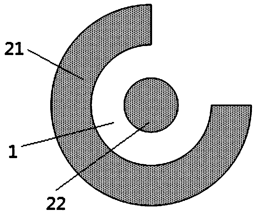
[0054] The P-type guard ring bipolar transistor structure of the present invention includes an N-type epitaxial layer 1 and a silicon dioxide insulating layer 3 arranged sequentially from bottom to top, and a P-type collector region 21 and a P-type Emitting region 22, P-type collector region 21 and P-type emitter region 22 are arranged concentrically, the depth of P-type collector region 21 and P-type emitter region 22 is the same, and P-type collector region 21 and P-type emitter region 22 are arranged There is an N-type base loop 5.

[0055] Among them, the lateral PNP transistor adopts a circular emitter region with a diameter of 6 μm, and a 30°-360° circular collector region with an inner diameter of 15 μm and an outer diameter of 27 μm. If the angle is less than 30°, the efficiency of the lateral PNP transistor is too low to be practical. The width of the base ring is 2.5 μm, the distance between the inner side of the base ring and the emitter region of the lateral PNP tr...


PUM

PropertyMeasurementUnit
Central angleaaaaaaaaaa

Abstract

The invention discloses a base region ring-doped anti-radiation lateral PNP transistor and a preparation method thereof. According to the invention, after a lateral PNP transistor structure is formedconventionally, N-type impurity injection is carried out on the surface of an N-type base region of the lateral PNP transistor once through a photoresist masking injection method, an annular N+ dopedregion is formed on the surface of the N-type base region, and the position where the width Wb of the base region of the lateral PNP transistor is located is pushed into an N-type epitaxial layer bodyfrom the surface of the N-type epitaxial layer. When the lateral PNP transistor with the base region being of a ring structure is in a total dose irradiation environment, although accumulation of positive charges in an oxide layer causes depletion and inversion of a P-type collector region and depletion and inversion of the surface of a P-type emitter region, the width of the base region of the lateral PNP transistor is not affected due to the fact that the width Wb of the base region is moved downwards to the position below the depletion and inversion of the P-type collector region and the depletion and inversion of the surface of the P-type emitter region, so that the lateral PNP transistor with the base region being of the ring structure has high total dose radiation resistance.

Description

technical field [0001] The invention belongs to the technical field of PNP transistors, and in particular relates to a base ring doped radiation-resistant lateral PNP transistor and a preparation method thereof. Background technique [0002] The lateral PNP transistor is a transistor structure often used in bipolar integrated circuits. In the production of traditional bipolar integrated circuits, the diffusion process or ion implantation process is used to do the P-type impurity doping of the collector and emitter regions of the lateral PNP transistor, namely Selective P-type impurity doping is carried out on the N-type epitaxial layer to form the P-type collector region and P-type emitter region of the lateral PNP transistor. The epitaxial layer is used as the N-type base region of the lateral PNP transistor, and the lateral PNP is finally realized through the leads. In the transistor structure, a layer of silicon dioxide is covered on the surface of the transistor as an in...

Claims


Application Information

Patent Timeline
IPC IPC(8): H01L29/735H01L29/10H01L29/06H01L21/331
CPCH01L29/735H01L29/1008H01L29/0684H01L29/6625
Inventor 赵杰薛东风薛智民孙有民王清波卓青青杜欣荣
Owner XIAN MICROELECTRONICS TECH INST
Why Eureka
Try Eureka