System for parallelly processing microporous texture of mechanical sealing face by femtosecond laser
A technology of femtosecond laser and processing machinery, applied in the field of femtosecond laser application, can solve the problems of low processing efficiency and slow speed, and achieve the effect of improving efficiency, good uniformity and good working conditions
- Summary
- Abstract
- Description
- Claims
- Application Information
AI Technical Summary
Problems solved by technology
Method used
Image
Examples
Embodiment 1
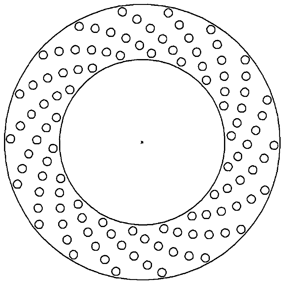
[0050] Example 1: A circular microporous texture with helical distribution is processed on a silicon carbide sealing device, and the schematic diagram of the texture to be processed is as follows figure 2 shown.
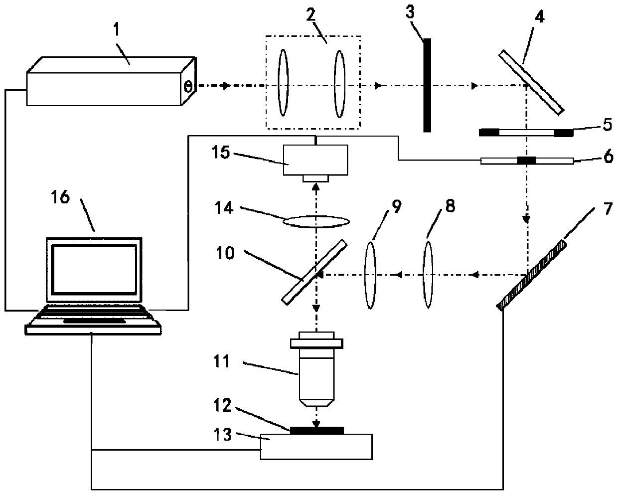
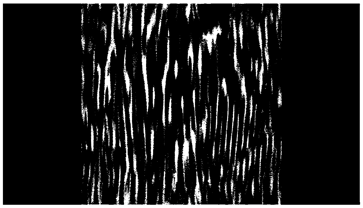
[0051] The specific processing steps of the present embodiment 1 are: turn on the femtosecond laser 1, and place the optical element according to figure 1 Installed as shown. When the correction lens group 2 is adjusted, the direction of the femtosecond laser coincides with the optical axis of the lens, that is, the beam can irradiate the sealing device 12 to be processed. Adjust the attenuation sheet 3 so that the laser power is 2mW. Adjust the aperture 5 so that the diameter of the laser beam is 7mm. The position of the six-dimensional translation stage 13 is adjusted by the computer 16 so that the sealing device 12 to be processed is on the focal plane of the objective lens 11 . followed by image 3 The phase map is loaded into the spatial light modulator 7 ...
Embodiment 2
[0052] Example 2: Processing a triangular microporous texture with helical distribution on the tungsten carbide sealing device, the schematic diagram of the texture to be processed is as follows Figure 5 shown.
[0053] The specific processing steps of the present embodiment 2 are: turn on the femtosecond laser 1, and place the optical element according to figure 1 Installed as shown. When the correction lens group 2 is adjusted, the direction of the femtosecond laser coincides with the optical axis of the lens, that is, the beam can irradiate the sealing device 12 to be processed. Adjust the attenuation sheet 3 so that the laser power is 4mW. Adjust the aperture 5 so that the diameter of the laser beam is 8mm. The position of the six-dimensional translation stage 13 is adjusted by the computer 16 so that the sealing device 12 to be processed is on the focal plane of the objective lens 11 . followed by Image 6 The phase map is loaded into the spatial light modulator 7 t...
Embodiment 3
[0054] Example 3: Processing the microporous groove texture on the silicon carbide sealing device, the schematic diagram of the texture to be processed is as follows Figure 8 shown.
[0055] The specific processing steps of the present embodiment 2 are: turn on the femtosecond laser 1, and place the optical element according to figure 1 Installed as shown. When the correction lens group 2 is adjusted, the direction of the femtosecond laser coincides with the optical axis of the lens, that is, the beam can irradiate the sealing device 12 to be processed. Adjust the attenuation sheet 3 so that the laser power is 2mW. Adjust the aperture 5 so that the diameter of the laser beam is 7 mm. The position of the six-dimensional translation stage 13 is adjusted by the computer 16 so that the sealing device 12 to be processed is on the focal plane of the objective lens 11 . followed by Figure 9 The phase map of the phase is loaded onto the spatial light modulator 7 through the con...
PUM
 Abstract
Description
Claims
Application Information


