High-impedance film and preparation method thereof

A high-impedance, sputtering technology, applied in metal material coating process, vacuum evaporation plating, coating, etc., can solve the problems of poor anti-interference effect, small surface resistance, poor anti-static effect, etc., to improve clarity Harmony, good anti-interference effect, good anti-static effect

Pending Publication Date: 2020-03-17
天津美泰真空技术有限公司
View PDF6 Cites 0 Cited by
  • Summary
  • Abstract
  • Description
  • Claims
  • Application Information

AI Technical Summary

Problems solved by technology

However, the performance of the current high-impedance film is average, especially when it is applied to a touch screen, or the surface resistance is small, the anti-interference effect is poor, or the anti-static effect is poor, which limits the use effect of the touch screen.

Method used


Image

  • High-impedance film and preparation method thereof
  • High-impedance film and preparation method thereof
  • High-impedance film and preparation method thereof

Examples


Embodiment 1

[0019] A method for preparing a high-impedance film, the method comprising the steps of:

[0020] The magnetron sputtering method is used to coat the glass substrate, the target used is an indium tin oxide ceramic target, and the pressure of the sputtering chamber is pumped to 1.5×10 -3 Pa, the working gas is argon, the concentration of argon is 99.99%, the sputtering pressure is 0.3Pa, the sputtering time is 2min, the sputtering power is 40W, the sputtering distance is 8cm, and the sputtering method is DC sputtering.

Embodiment 2

[0022] A method for preparing a high-impedance film, the method comprising the steps of:

[0023] The magnetron sputtering method is used to coat the glass substrate, the target material used is an indium tin oxide ceramic target, and the pressure of the sputtering chamber is pumped to 2×10 -3 Pa, the working gas is argon, the concentration of argon is 99.99%, the sputtering pressure is 0.6Pa, the sputtering time is 7min, the sputtering power is 80W, the sputtering distance is 8cm, and the sputtering method is DC sputtering.

Embodiment 3

[0025] A method for preparing a high-impedance film, the method comprising the steps of:

[0026] The magnetron sputtering method is used to coat the glass substrate, the target used is an indium tin oxide ceramic target, and the pressure of the sputtering chamber is pumped to 3×10 -3 Pa, the working gas is argon, the concentration of argon is 99.99%, the sputtering pressure is 1.0Pa, the sputtering time is 10min, the sputtering power is 100W, the sputtering distance is 8cm, and the sputtering method is DC sputtering.

[0027] The square resistance of the high resistance film that embodiment 1-3 makes is 10 8 -10 10 Europe.

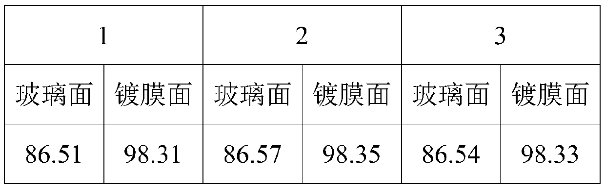
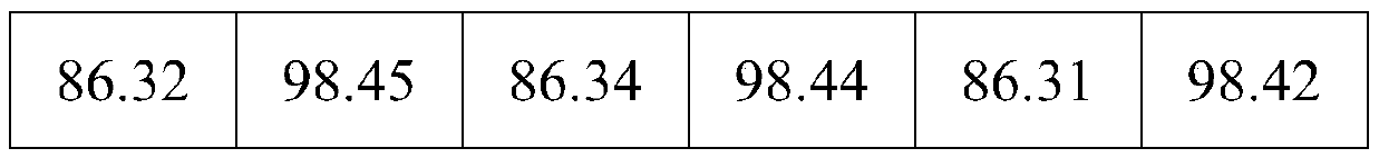
[0028] Take three pieces of 5cm×5cm coated glass prepared in Examples 1-3 respectively, and measure the transmittance values ​​before and after the coated glass under sunlight and the square resistance values, as shown in Table 1-Table 3.

[0029] Table 1 embodiment 1 makes the transmittance of coated glass

[0030]

[0031] Table 2 embodiment 1 m...


PUM

PropertyMeasurementUnit
thicknessaaaaaaaaaa
electrical resistanceaaaaaaaaaa

Abstract

The invention provides a preparation method of a high-impedance film. The method comprises the following steps: a magnetron sputtering method is adopted to coat a glass substrate with a film, the usedtarget material is an indium-containing composite material, the pressure of a sputtering chamber is pumped to 1.5-3.5*10<-3>Pa, the working gas is argon, and the sputtering pressure is 0.3-1.0 Pa. The high-impedance film disclosed by the invention has a relatively high surface resistance value, a relatively good anti-static effect and a relatively good anti-interference effect.

Description

technical field [0001] The invention relates to the technical field of thin films, in particular to a high-resistance film and a preparation method thereof. Background technique [0002] The high-resistance film with high-impedance characteristics is widely used and can be used in electronic devices. When the high-resistance film is grounded, it can shield the electronic device from static electricity, and it can also be used in liquid crystal displays as a control element to control conduction in certain directions. , disconnected in some directions, can also be used as electrodes. However, the performance of the current high-impedance film is average, especially when it is applied to a touch screen, or the surface resistance is small, the anti-interference effect is poor, or the anti-static effect is poor, which limits the use effect of the touch screen. Contents of the invention [0003] In view of this, the present invention aims to propose a high-impedance film with ...

Claims


Application Information

Patent Timeline
Patent Type & Authority Applications(China)
IPC IPC(8): C23C14/35C23C14/08
CPCC23C14/35C23C14/086
Inventor 夏伟张兵郑建军张成金姚仕军方添志赵帅
Owner 天津美泰真空技术有限公司
Why Eureka
Try Eureka