Output stage circuit of high-side switch
An output stage circuit, high-side switch technology, applied in circuits, electronic switches, electrical components, etc., can solve problems such as inability to accurately limit PMOS power transistor M1, low loop gain, and excessive breakdown of gate oxide layers. , to achieve the effect of saving the layout area
- Summary
- Abstract
- Description
- Claims
- Application Information
AI Technical Summary
Problems solved by technology
Method used
Image
Examples
Embodiment Construction
[0030] Below in conjunction with accompanying drawing and specific embodiment, describe technical solution of the present invention in detail:
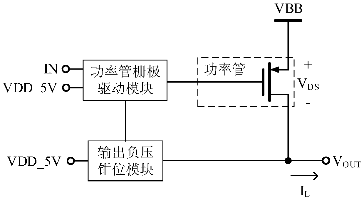
[0031] Such as image 3 Shown is a schematic diagram of the output stage circuit principle of a high-side switch proposed by the present invention. The high-side switch adopts a PMOS power transistor, and the output stage circuit includes a power transistor gate drive module and an output negative voltage clamp module. The power tube gate drive module is used to control the switching of the power tube under all circumstances, and to ensure the gate-source voltage |VGS| of the power tube within a limited range, so as to avoid the breakdown of the gate oxide layer of the power tube. When the power tube is turned off, the output negative pressure clamping module starts to work, and pulls down the grid potential of the power tube, so that the power tube is turned on and the current of the power tube is equal to the current of the inductor...
PUM
 Abstract
Description
Claims
Application Information


