Method for preparing crystal diode based on soluble protective film

A protective film and diode technology, which is applied in the manufacture of electric solid-state devices, semiconductor devices, semiconductor/solid-state devices, etc., can solve problems such as the reduction of diode finishing yields, reduce plugging and grinding steps, improve yields, and reduce cost effect

Pending Publication Date: 2020-04-07
LIZ ELECTRONICS KUNSHAN
View PDF0 Cites 0 Cited by
  • Summary
  • Abstract
  • Description
  • Claims
  • Application Information

AI Technical Summary

Problems solved by technology

With the development of miniaturization of electronic components, limited by the precision achieved by existing processes, the finishing yield of the manufactured diodes is reduced.

Method used


Image

  • Method for preparing crystal diode based on soluble protective film
  • Method for preparing crystal diode based on soluble protective film
  • Method for preparing crystal diode based on soluble protective film

Examples


Embodiment Construction

[0029] In order to make the object, technical solution and advantages of the present invention more clear, the present invention will be further described in detail below in conjunction with the examples. It should be understood that the specific embodiments described here are only used to explain the present invention, not to limit the present invention.

[0030] The application principle of the present invention will be described in detail below in conjunction with the accompanying drawings.

[0031] Implement the method in the present invention to prepare the material of the used raw material of crystal diode:

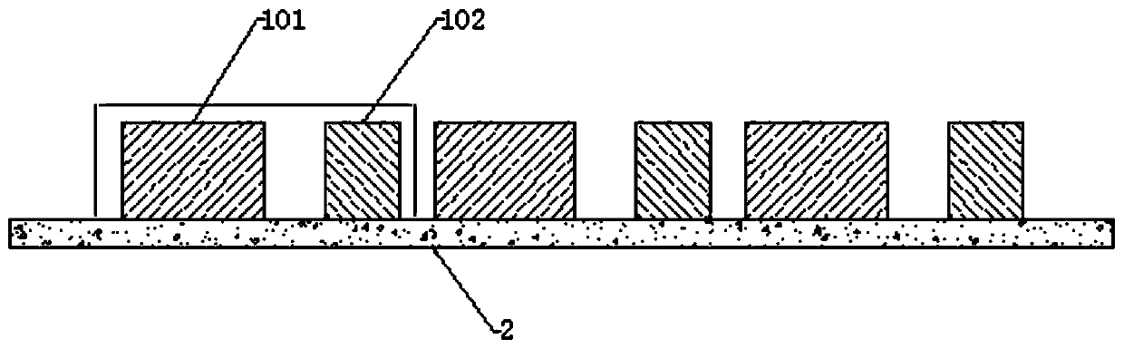
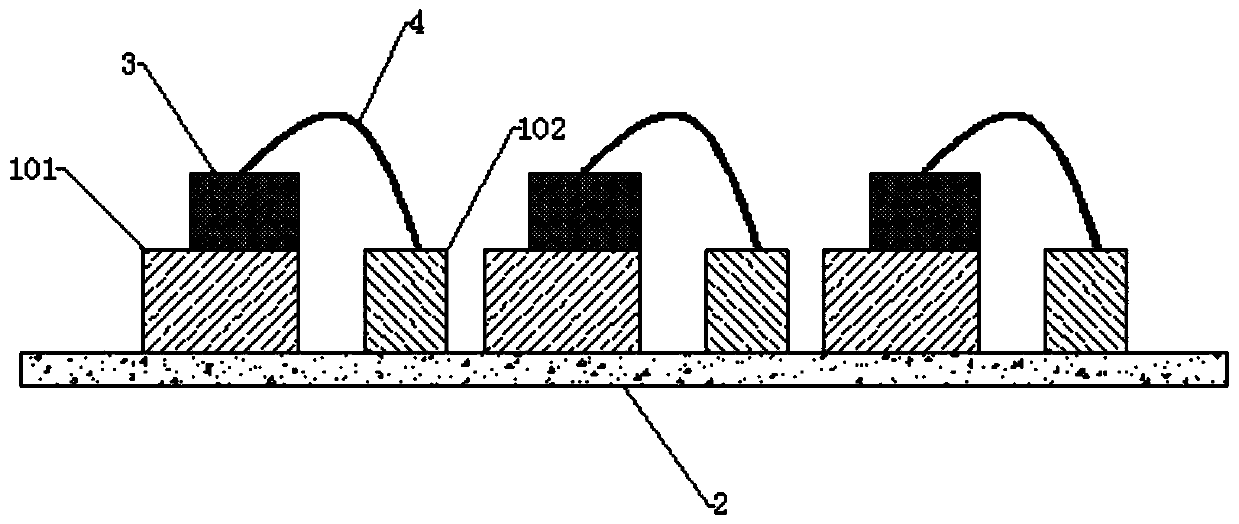
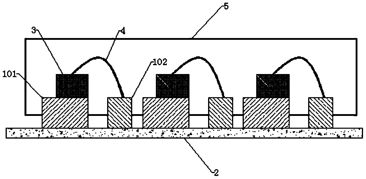
[0032] Substrate: Fiberglass board

[0033] Wire: gold, copper, aluminum, silver

[0034] Protective film: 0.2mm thick film layer composed of polyethylene.

[0035] Encapsulation layer: epoxy resin layer

[0036] An embodiment of the present invention provides a method for manufacturing a diode device with a substrate with a dry film, including:

[0037] (1) Et...


PUM


Abstract

The invention discloses a method for preparing a crystal diode based on a soluble protective film, which comprises the following steps: (1) substrate treatment: etching corresponding areas on the front surface and the back surface of a substrate to form an etching area, wherein the substrate comprises a substrate A and a substrate B; (2) attachment of a protective film: placing the plurality of paired substrates A and substrates B obtained in the step (1) on the protective film in a matrix arrangement form, and attaching the back surfaces of the substrates to the protective film; (3) preparation of a diode semi-finished product; (4) removing of the protective film: dissolving the protective film by adopting an organic solvent; and (5) preparation of a diode finished product: cutting the packaging layer into particles. According to the invention, through the design of pasting the protective film on the back surface of the substrate, the problem that the packaging adhesive permeates intothe back electrode of the substrate can be completely prevented, the limitation of the size to the precision is reduced, and the miniaturization development of the manufactured crystal diode is facilitated.

Description

technical field [0001] The invention belongs to the field of crystal diodes, in particular to a method for preparing crystal diodes based on a soluble protective film. Background technique [0002] In the existing traditional diode manufacturing process, the required glass fiber substrate is usually manufactured by etching, drilling, plugging, and grinding. With the development of miniaturization of electronic components, limited by the precision achieved by the existing technology, the finishing yield of the manufactured diodes is reduced. Contents of the invention [0003] In view of the above problems, the present invention proposes a method for preparing a crystal diode based on a soluble protective film. [0004] Realize above-mentioned technical purpose, reach above-mentioned technical effect, the present invention realizes through the following technical solutions: [0005] A method for preparing a crystal diode based on a soluble protective film, comprising the f...

Claims


Application Information

Patent Timeline
IPC IPC(8): H01L21/67H01L21/683H01L21/78
CPCH01L21/67132H01L21/6836H01L21/78H01L2221/6834
Inventor 邓月忠温国豪褚宏深宋旭官黄正信
Owner LIZ ELECTRONICS KUNSHAN
Why Eureka
Try Eureka