Input buffer circuit based on GaAs process
A technology of input buffer circuit and process, which is applied in the direction of logic circuit coupling device, logic circuit interface device, logic circuit connection/interface layout, etc., can solve the problems affecting the working state of the circuit, and achieve the effect of strong versatility
- Summary
- Abstract
- Description
- Claims
- Application Information
AI Technical Summary
Problems solved by technology
Method used
Image

Examples
Embodiment Construction
[0021] The technical solutions and beneficial effects of the present invention will be described in detail below in conjunction with the accompanying drawings.
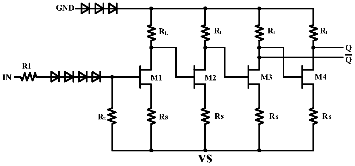
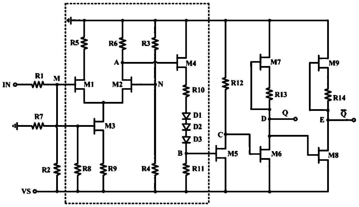
[0022] like figure 2 As shown, the present invention provides an input buffer circuit based on a GaAs process, including a first PHEMT tube M1, a second PHEMT tube M2, a third PHEMT tube M3, a fourth PHEMT tube M4, a fifth PHEMT tube M5, and a sixth PHEMT tube. Tube M6, seventh PHEMT tube M7, eighth PHEMT tube M8, ninth PHEMT tube M9, first resistor R1, second resistor R2, third resistor R3, fourth resistor R4, fifth resistor R5, sixth resistor R6 , the seventh resistor R7, the eighth resistor R8, the ninth resistor R9, the tenth resistor R10, the eleventh resistor R11, the twelfth resistor R12, the thirteenth resistor R13, the fourteenth resistor R14, the first Schottky Diode D1, second Schottky diode D2 and third Schottky diode D3;
[0023] The source of the first PHEMT transistor M1 is respectively connected to ...
PUM
 Abstract
Description
Claims
Application Information
 - R&D
- Intellectual Property
- Life Sciences
- Materials
- Tech Scout
- Unparalleled Data Quality
- Higher Quality Content
- 60% Fewer Hallucinations
Browse by: Latest US Patents, China's latest patents, Technical Efficacy Thesaurus, Application Domain, Technology Topic, Popular Technical Reports.
© 2025 PatSnap. All rights reserved.Legal|Privacy policy|Modern Slavery Act Transparency Statement|Sitemap|About US| Contact US: help@patsnap.com