Method for cutting silicon wafer in thinning manner

A technology for thinning silicon wafers and cutting silicon wafers. It is applied to fine working devices, grinding machines, and working accessories. It can solve problems such as poor performance of silicon wafers, large vibration amplitude of diamond wires, and uneven thickness of silicon wafers. , to achieve the effect of low surface roughness and damaged layer thickness, short cutting time, and less loss of silicon material

Inactive Publication Date: 2020-04-17
TIANJIN HUANOU SEMICON MATERIAL TECH CO LTD
View PDF8 Cites 4 Cited by
  • Summary
  • Abstract
  • Description
  • Claims
  • Application Information

AI Technical Summary

Problems solved by technology

[0003] Most of the diamond wire diameters currently used are between 60 and 80um. In addition, the vibration of the diamond wire is large during the cutting process, which makes the surface of the silicon wafer obtained by cutting rough and the thickness of the damaged layer is high, especially in the knife-entry area. The thickness of the silicon wafer in the cutting area is very uneven, so the average TTV (total thickness deviation) of the silicon wafer is as high as about 20um, resulting in poor performance of the silicon wafer; and the loss of silicon material during the cutting process greatly increases the overall cost.

Method used


Image

  • Method for cutting silicon wafer in thinning manner

Examples


Embodiment Construction

[0018] The present invention will be further explained below in conjunction with the drawings.

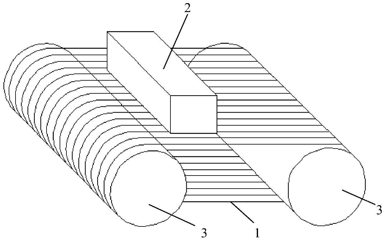
[0019] The invention discloses a method for cutting thin wire silicon wafers. The method adopts a diamond wire 1 with a diameter of 45um for cutting, and during the cutting process, the acceleration of the diamond wire 1 is 5m / s 2 -9m / s 2 , The operating speed is 800m / min-2000m / min; the tension of the diamond wire 1 is 6N-13N; the downward movement speed of the silicon material 2 is set as: the cutting area 0.5mm / min -1.5mm / min; the main cutting area 1.6 mm / min-2.8mm / min; cutting area 0.2mm / min-1.0mm / min.

[0020] The acceleration of the diamond wire 1 can be set to 6m / s 2 Or 8m / s 2 .

[0021] The operating speed of the diamond wire 1 can be set to 1000 m / min or 1200 m / min or 1500 m / min or 1800 m / min.

[0022] The tension of the diamond wire 1 can be set to 8N or 10N.

[0023] During the cutting process, the grooved wheel 3 reciprocates to drive the diamond wire 1 into a saw-like reciprocat...


PUM


Abstract

The invention provides a method for cutting a silicon wafer in a thinning manner. The method adopts a diamond line with the diameter of 45 [mu]m for cutting, and in the cutting process, the acceleration of the diamond line is 5m / s<2>-9m / s<2>, the running speed is 800m / min-2000m / min, and the tension of the diamond line is 6N-13N; and the downward moving speed of a silicon material is set as follows: the cutting speed of a cutter entering area is 0.5mm / min-1.5mm / min, the cutting speed of a main cutting area is 1.6mm / min-2.8mm / min, and the cutting speed of a cutter retracting area is 0.2mm / min-1.0 mm / min. When the method is adopted for cutting the silicon wafer, the surface roughness and the thickness of a damaged layer of the obtained silicon wafer are low, the TTV mean value of the siliconwafer is low, and the performance of the silicon wafer is good; and in the cutting process, the loss of the silicon material is less, the wafer yield is high, and the cutting time of the silicon material with the same size is shorter, so that the cost is effectively reduced.

Description

Technical field [0001] The invention relates to the technical field of silicon wafer cutting, in particular to a method for thin-line silicon wafer cutting. Background technique [0002] Silicon wafers are widely used in photovoltaic solar energy, liquid crystal display and semiconductor fields, so wafer cutting technology has also developed rapidly. At present, the cutting of crystalline silicon wafers mainly adopts multi-wire cutting technology. Multi-wire cutting is a new type of silicon wafer cutting technology that has been developed and matured in recent years. Its principle is that diamond wires are wound on two grooved wheels of the slicing machine to form a multi-line shape. The wire mesh, the groove wheel reciprocates at a high speed, thereby driving the diamond wire saw-type reciprocating high-speed operation, and the silicon material moves down under the control of the control device to contact the high-speed diamond wire, passing through the diamond wire and the sili...

Claims


Application Information

Patent Timeline
Patent Type & Authority Applications(China)
IPC IPC(8): B28D5/04B28D7/02B24B27/06
CPCB24B27/0633B28D5/0076B28D5/045
Inventor 张中赛王少刚付少华魏辉杜晓玮古元甲邱长兴李方乐张悦吕志刚辛超危晨李建弘范猛史丹梅
Owner TIANJIN HUANOU SEMICON MATERIAL TECH CO LTD
Why Eureka
Try Eureka