Semiconductor device and preparation method thereof

A semiconductor and device technology, applied in the field of semiconductor devices and their preparation, can solve the problems of carrier mobility reduction, signal transmission distortion, affecting device linearity, etc., and achieve the effect of improving interface scattering effect and uniform gate voltage change

Active Publication Date: 2020-04-21
DYNAX SEMICON
View PDF2 Cites 0 Cited by
  • Summary
  • Abstract
  • Description
  • Claims
  • Application Information

AI Technical Summary

Problems solved by technology

[0003] The most important advantage of AlGaN / GaN HEMT (High Electron Mobility Transistor, High Electron Mobility Transistor) is that it is suitable for high-frequency, high-power microwave devices and has great application prospects. These extensive application prospects are mainly due to the With the increase of the dynamic range of the signal, the linearity requirements of the power amplifier in the base station circuit are also getting higher and higher, but the transconductance of the traditional AlGaN / GaN HEMT structure presents a typical peak characteristic, that is, the transconductance will be seriously damaged under high current. degraded, resulting in distorted signal transmission
Some studies have shown that: under high field, the scattering of the material interface will lead to the reduction of carrier mobility, thereby affecting the linearity of the device, and the speed of the change of the carrier concentration in the channel under the device gate with the gate voltage will also affect the device. linearity

Method used


Image

  • Semiconductor device and preparation method thereof
  • Semiconductor device and preparation method thereof
  • Semiconductor device and preparation method thereof

Examples


Embodiment 1

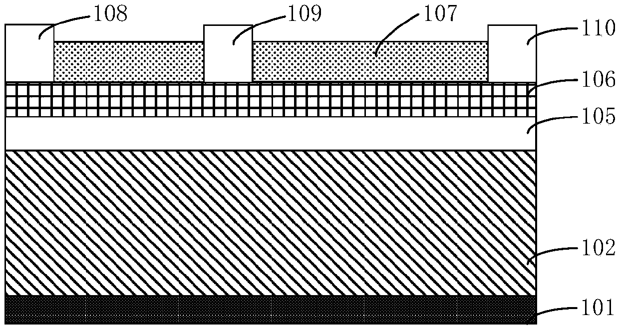
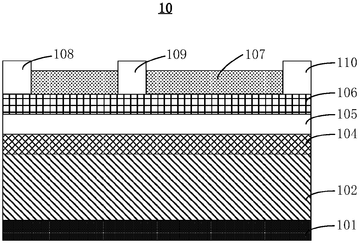
[0048] In order to solve the above problems, the embodiment of the present application provides a semiconductor device 10, such as image 3 As shown, the semiconductor device 10 includes a substrate 101 , a buffer layer 102 , a transition layer 104 , a channel layer 105 , a barrier layer 106 , a passivation layer 107 , a source 108 , a gate 109 and a drain 110 .

[0049] In detail, the substrate 101 may be made of sapphire (Sapphire), silicon carbide (SiC), silicon (Si), lithium niobate, rare earth oxide or any other suitable material. Optionally, the substrate 101 may be made of silicon carbide with good heat dissipation properties.

[0050] The material of the buffer layer 102 may be nitride, specifically GaN or AlN or other nitrides, and the buffer layer 102 may be used to match the material of the substrate 101 with the epitaxial transition layer 104 and the channel layer 105 .

[0051]Generally speaking, the semiconductor layer includes a channel layer 105 and a barrier ...

Embodiment 2

[0057] In another embodiment, in order to improve the confinement of electrons in the channel, further improve its linearity, such as Figure 5 As shown, a back barrier layer 103 is formed on the side of the transition layer 104 close to the substrate 101. In the embodiment of the present application, a back barrier layer 103 is formed between the transition layer 104 and the nitride buffer layer 102. The barrier layer 103 is used to increase the energy level difference between the transition layer 104 and the buffer layer 102, thereby forming a square-like electron movement channel with a certain width. The band gap of the back barrier layer 103 is greater than the band gap of the transition layer 104 , preferably, the band gap of the back barrier layer 103 is greater than the band gap of the transition layer 104 and the channel layer 105 . The back barrier layer 103 may be made of at least one material among aluminum gallium nitride (AlGaN), aluminum nitrogen (AlN), gallium ...

Embodiment 3

[0060] The embodiment of the present application also provides a method for preparing a semiconductor device, such as Figure 7 shown, including the following steps.

[0061] Step S101, providing a substrate.

[0062] Step S102, fabricating a buffer layer based on the substrate.

[0063] The embodiment of the present application does not limit the material of the substrate, and the buffer layer may be formed by depositing materials such as GaN or InGaN on the surface of the substrate.

[0064] Step S103, forming a transition layer on the side of the buffer layer away from the substrate.

[0065] In the embodiment of this application, after the buffer layer is formed, gallium nitride or indium gallium nitride can also be deposited on the surface of the buffer layer to form a transition layer. The transition layer can be heavily doped with n-type, and its doping concentration can be greater than 1e17cm -3 .

[0066] Preferably, in step S104, before forming the transition lay...


PUM


Abstract

The invention provides a semiconductor device and a preparation method thereof, and relates to the technical field of semiconductors. According to the semiconductor device in the embodiment of the invention, an epitaxial structure of the device is adjusted to modulate electron concentration distribution of a traditional device so as to change the traditional electron concentration peak position, the electron concentration peak position in the semiconductor layer is moved from the interface of a channel layer and a barrier layer to the direction close to a transition layer, and electron distribution functions in the semiconductor channel layer are overlapped, more discrete energy levels which can be occupied by electrons are formed in a channel potential well, and finally, the channel potential well is expanded into a quasi-square electron channel potential well with a certain width, so that the performance such as the linearity of the device is effectively improved.

Description

technical field [0001] The invention relates to the technical field of semiconductors, in particular to a semiconductor device and a preparation method thereof. Background technique [0002] GaN (gallium nitride) semiconductor devices have significant advantages such as large band gap, high electron mobility, high breakdown field strength, and high temperature resistance. Compared with the first-generation semiconductor silicon and the second-generation semiconductor gallium arsenide, it is more suitable It has broad application prospects for making high-temperature, high-voltage, high-frequency and high-power electronic devices. [0003] The most important advantage of AlGaN / GaN HEMT (High Electron Mobility Transistor, High Electron Mobility Transistor) is that it is suitable for high-frequency, high-power microwave devices and has great application prospects. These extensive application prospects are mainly due to the With the increase of the dynamic range of the signal, ...

Claims


Application Information

Patent Timeline
IPC IPC(8): H01L29/778H01L21/335
CPCH01L29/778H01L29/66431
Inventor 张乃千刘健
Owner DYNAX SEMICON
Why Eureka
Try Eureka