Super-structure honeycomb composite wave-absorbing material
A composite wave absorbing material and superstructure technology, applied in the field of wave absorbing materials, can solve the problem that the stealth frequency band of the honeycomb stealth material is not wide enough, and achieve the effect of excellent broadband/low frequency wave absorbing performance and excellent mechanical bearing capacity.
- Summary
- Abstract
- Description
- Claims
- Application Information
AI Technical Summary
Problems solved by technology
Method used
Image
Examples
Embodiment 1
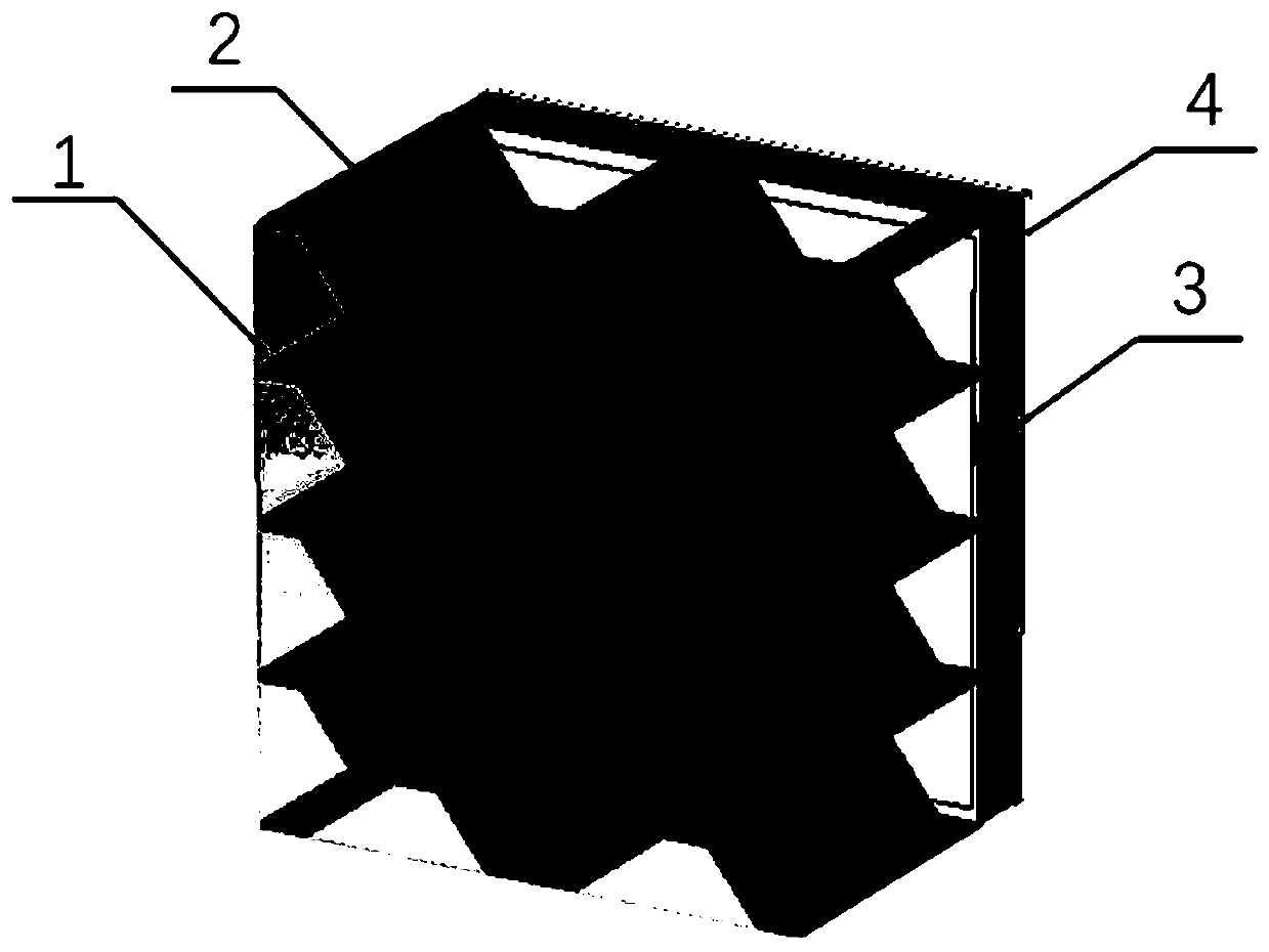
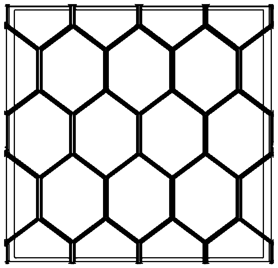
[0024] (1) Weigh 25 parts of wave-absorbing agent, 40 parts of epoxy resin and curing agent, 35 parts of phenolic resin, add appropriate amount of diluent and mix to make wave-absorbing slurry, and evenly impregnate it on the surface of aramid honeycomb. High temperature drying, high temperature 130 degrees curing. Repeat the above operation several times to obtain the aramid wave-absorbing honeycomb;
[0025] (2) In the form of a printed circuit board, a metamaterial array is printed on a 1.1mm thick epoxy resin board. The metamaterial array is an array composed of copper squares with a side length of 10mm, and the distance between the copper squares in the array is 1mm. Prepared metamaterial wave-absorbing layer;
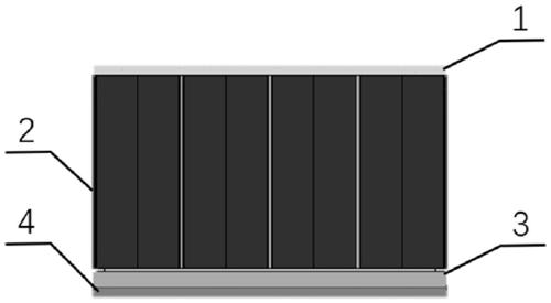
[0026] (3) The wave-transparent skin layer, the aramid wave-absorbing honeycomb, the metamaterial wave-absorbing layer, and the metal back plate are bonded in sequence with epoxy resin adhesive. A wave-absorbing material composited with a honeycomb structure and...
Embodiment 2
[0028] (1) Weigh 15 parts of wave-absorbing agent, 100 parts of epoxy resin and curing agent according to parts by mass, add appropriate amount of diluent and mix to make wave-absorbing slurry, which is evenly impregnated on the surface of aramid honeycomb, dried at low temperature at 60 degrees, and dried at high temperature Curing at 120 degrees. Repeat the above operation several times to obtain the aramid wave-absorbing honeycomb;
[0029] (2) In the form of a printed circuit board, the metamaterial array is printed on a 2mm thick epoxy resin board. The metamaterial array is an array composed of copper back-shaped units with a side length of 30mm. The outer side length of the unit in the array is is 30mm, the side length of the inner square is 15mm, and the cell spacing in the array is 3mm;
[0030] (3) The wave-transparent skin layer, the aramid wave-absorbing honeycomb, the metamaterial wave-absorbing layer, and the metal back plate are bonded in sequence with epoxy res...
Embodiment 3
[0032] (1) According to the mass, 10 parts of surfactant-treated wave-absorbing agent, 100 parts of phenolic resin, mixed with an appropriate amount of diluent to make a wave-absorbing slurry, uniformly impregnated on the surface of the aramid honeycomb, dried at low temperature, and cured at high temperature. Repeat the above operation several times to obtain the desired wave-absorbing honeycomb.
[0033] (2) In the form of a printed circuit board, a metamaterial array is printed on a 2.5mm thick epoxy resin board. The units in the array are cross-shaped, the outer length of the unit is 25mm, and the unit spacing is 2mm.
[0034] (3) The skin wave-transmitting layer, the honeycomb structure layer, the metamaterial wave-absorbing layer, and the metal back plate are bonded in sequence with epoxy resin adhesive. A wave-absorbing material composited with a honeycomb structure and a metamaterial structure is obtained.
[0035] The present invention combines the metamaterial absor...
PUM
 Abstract
Description
Claims
Application Information


