Nickel target blank and manufacturing method of target material

A manufacturing method and nickel target material technology, which is applied in metal material coating process, ion implantation plating, coating, etc., can solve the problems of nickel target blank defects, material waste, etc.

Inactive Publication Date: 2020-05-01
KONFOONG MATERIALS INTERNATIONAL CO LTD
View PDF5 Cites 9 Cited by
  • Summary
  • Abstract
  • Description
  • Claims
  • Application Information

AI Technical Summary

Problems solved by technology

[0005] The problem solved by the present invention is that existi

Method used


Image

  • Nickel target blank and manufacturing method of target material
  • Nickel target blank and manufacturing method of target material
  • Nickel target blank and manufacturing method of target material

Examples


Embodiment Construction

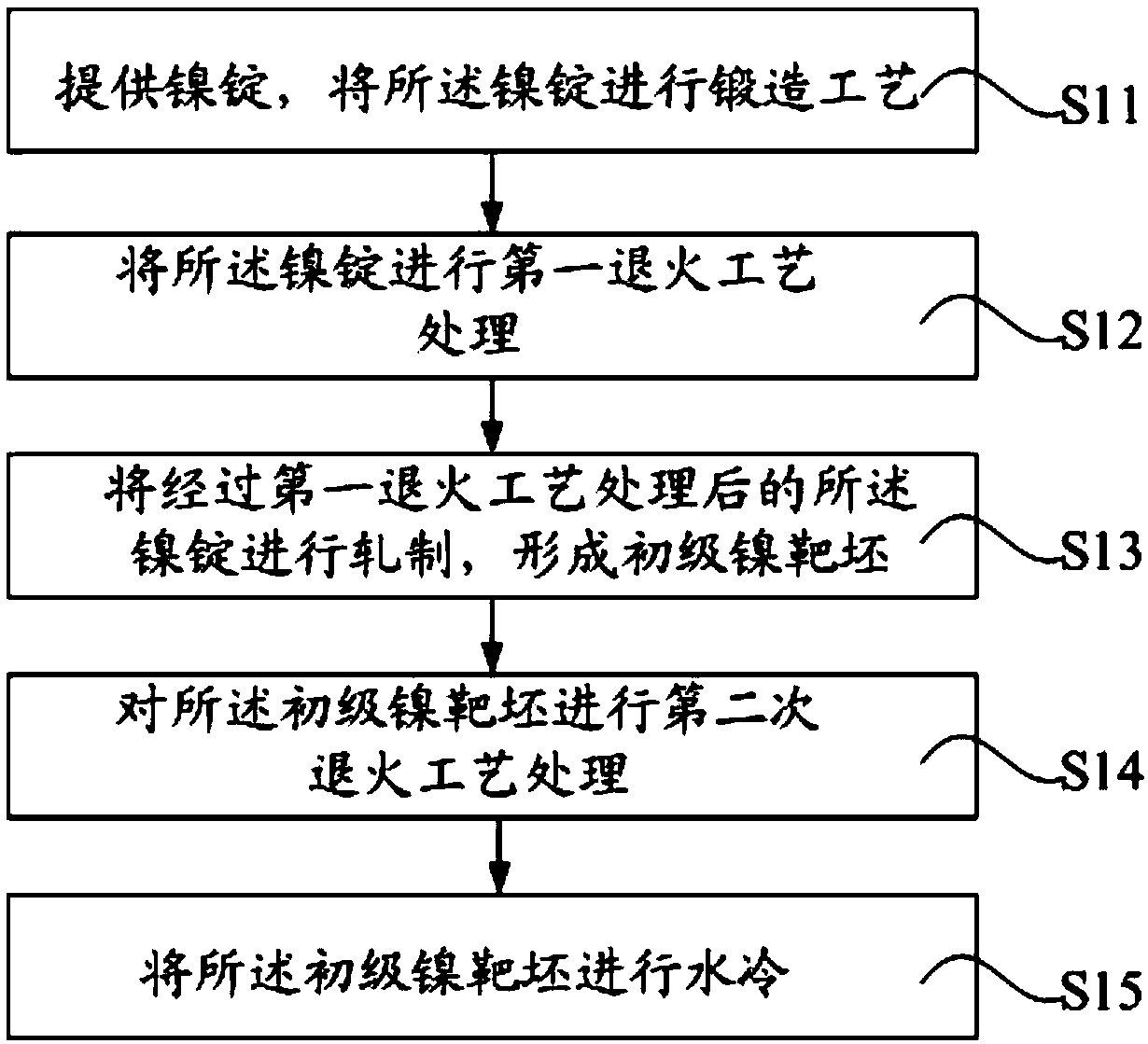
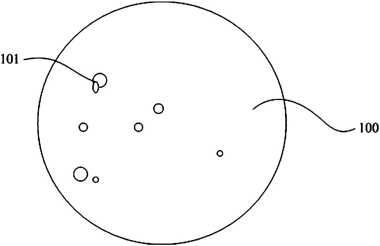
[0027] It can be seen from the background technology that in the prior art, the manufactured nickel target blanks are often easy to get gas and generate inclusions during the manufacturing process, and the formed nickel target blanks have defects, which are not satisfied with the application in the semiconductor industry, resulting in material waste and increased costs.

[0028] Analysis shows that in the prior art, the method to make the manufactured nickel target meet the various parameters in the semiconductor industry is to strictly control the parameters in the annealing process after rolling. However, a large number of facts have proved that However, the defect of the manufactured nickel target blank cannot be completely overcome.

[0029] In order to solve the above problems, the present invention provides a new method, providing nickel ingots; performing the first annealing process on the nickel ingots, the temperature of the first annealing process is 900°C-950°C; Th...


PUM


Abstract

The invention discloses a nickel target blank and a manufacturing method of a target material. The manufacturing method of the nickel target blank comprises the following steps that a nickel ingot isprovided; the nickel ingot is subjected to first annealing process treatment, wherein the temperature of the first annealing process is 900-950 DEG C; and the nickel ingot treated by the first annealing process is rolled to form a primary nickel target blank. Before the nickel ingot is subjected to roll forming, the nickel ingot is subjected to primary annealing process treatment, so that the hardness of the nickel ingot material is reduced, so that the later cutting process is easier, residual stress in the nickel ingot is released, the deformation and cracking tendency of the material is reduced, and the effect of refining grains is achieved. The temperature of the first annealing process is controlled to be 900-950 DEG C, so that the interior of the rolled nickel target blank is free ofdefects, the nickel target material obtained after the nickel target blank is welded to a back plate is also free of defects, and the situation that the target material is scrapped due to the fact that the nickel target blank does not meet the requirement is reduced.

Description

technical field [0001] The invention relates to the preparation of a semiconductor sputtering target, in particular to a nickel target blank and a method for manufacturing the target. Background technique [0002] The sputtering target is an extremely important key material necessary for the manufacture of semiconductor chips. The principle is to use PVD (Physical Vapor Deposition Technology) to bombard the target with high-pressure accelerated gaseous ions, so that the atoms of the target are sputtered out to It is deposited on the silicon wafer in the form of a thin film, which eventually forms the complex wiring structure in the semiconductor chip. Sputtering targets have many advantages such as uniformity and controllability of metal coatings, and are widely used in the semiconductor field. The quality of PVD film mainly depends on the purity, microstructure and other factors of the sputtering target. With the rapid development of the semiconductor industry, the demand...

Claims


Application Information

Patent Timeline
IPC IPC(8): C23C14/34C22F1/10
CPCC22F1/10C23C14/3414
Inventor 姚力军潘杰王学泽黄东长
Owner KONFOONG MATERIALS INTERNATIONAL CO LTD
Why Eureka
Try Eureka